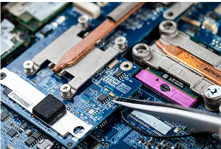
The main purpose of this IPC/JEDEC J-STD-020C is to test and classify moisture (moisture absorption) sensitivity for various non-hermetic SMT semiconductor components to remind the semiconductor industry to package, store, and follow-up. Pay attention to how to prevent moisture during use, in order to cope with the test of lead-free high-temperature soldering or heavy work, and reduce the strong stress caused by instant vaporization due to moisture absorption. This stress will cause the internal, interface or outer edge of the component to burst or crack, Which is the so-called "popcorn" phenomenon. As for the early DIP double row pin socket wave soldering package components, because the IC body does not directly face the heat source, but the pin soldering is performed away from the strong wave crest through the PCB, and this type of through-hole soldering is wave soldering IC is not under the jurisdiction of this specification.
1. About SMT original grading and examination procedures
(1) Classification and test welding depth

Since various SMD-type packaged components (not necessarily ICs, in solder paste welding, their bodies must directly face the heat source and are prone to cracking. Because other components of different sizes need to be mounted on the board respectively, it is For the sake of considering that all large parts must be welded properly, the setting of the reflow (warm time) curve will inevitably cause overheating for small parts, which often makes small and thick parts more likely to burst. That is, according to the thickness and size of the components, different reflow peak temperatures are configured to adapt to the reflow of different models.
The component supplier must be able to guarantee the compatibility of the manufacturing process for the certified components when they reach the grading temperatures listed here.
(1) When the tolerance of the reflow curve set by the production line according to the variable capacity is ten 0 degree Celsius and one X degree Celsius, in order to obtain good control of the temperature curve, the process change should not exceed 5 degree Celsius. Suppliers must ensure the process compatibility of their products at peak temperatures.
About SMT patch original grading and examination procedures
(2) The so-called package volume here also includes the pins outside the body and various additional heat sinks (such as balls, bumps, pads, pins, etc.).
(3) The maximum temperature that the component can reach during reflow is related to the thickness and volume of the component. The use of air (or nitrogen) convection heating heat source can reduce the heat drop between the components, but due to the difference in heat capacity of each SMD, the heat difference between them is still difficult to completely eliminate.
(4) Anyone who wants to adopt the assembly process of lead-free soldering must comply with the lead-free grading temperature and reflow temperature-time curve.
(2) Lead-free heavy industry (rework) capability
According to the above regulations, packaging components that can withstand lead-free soldering must be reworked below 260°C within 8 hours after leaving the dry box or oven.