The layout of components should be designed according to the characteristics and requirements of SMT chip processing production equipment and process. Different processes, such as reflow soldering and wave soldering, have different layouts of components. When double-sided reflow soldering, there are also different requirements for the layout of the A side and the B side; selective wave soldering and traditional wave soldering also have different requirements.
The basic requirements of SMT process for component layout design are as follows:
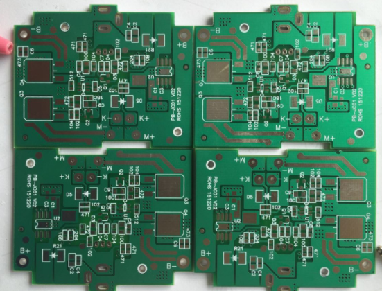
The distribution of components on the printed circuit board should be as uniform as possible. The heat capacity of large-mass components during reflow soldering is relatively large. Too much concentration can easily lead to low local temperature and lead to false soldering. At the same time, the uniform layout is also conducive to the balance of the center of gravity. In, it is not easy to damage the components, metallized holes and pads.
The arrangement direction of the components on the printed circuit board, similar components should be arranged in the same direction as much as possible, and the characteristic directions should be consistent to facilitate the placement, welding and testing of the components. For example, the anode of the electrolytic capacitor, the anode of the diode, the single-pin end of the triode, and the first pin of the integrated circuit are arranged in the same direction as possible. The printing orientation of all component numbers is the same.
The size of the heater head of the SMD rework equipment that can be operated shall be reserved around the large components.

Heating components should be as far away from other components as possible, generally placed in corners and in a ventilated position in the chassis. The heating components should be supported by other leads or other supports (such as heat sinks can be added) to keep the heating components and the surface of the printed circuit board at a certain distance. The minimum distance is 2mm. Heating components connect the heating component body with the printed circuit board in the multilayer board, and make metal pads during design, and connect them with solder during processing, so that the heat can be dissipated through the printed circuit board.
Temperature sensitive components should be kept away from heating components. For example, triodes, integrated circuits, electrolytic capacitors and some plastic shell components should be kept as far away as possible from bridge stacks, high-power components, radiators and high-power resistors.
The layout of components and parts that need to be adjusted or frequently replaced, such as potentiometers, adjustable inductance coils, variable capacitor microswitches, fuses, buttons, plug-ins and other components, should consider the structural requirements of the whole machine. Place it in a position where it is easy to adjust and replace. If it is adjusted inside the machine, it should be placed on the printed circuit board where it is easy to adjust; if it is adjusted outside the machine, its position should be adapted to the position of the adjustment knob on the chassis panel to prevent conflicts between the three-dimensional space and the two-dimensional space. For example, the panel opening of the toggle switch and the empty position of the switch on the printed circuit board should match.
Fixing holes should be provided near the terminals, plug-in parts, the center of long series of terminals, and the parts that are often subjected to force, and there should be corresponding space around the fixing holes to prevent deformation due to thermal expansion. If the thermal expansion of the long series of terminals is more serious than that of the printed circuit board, the phenomenon of warping is prone to occur during wave soldering.
Some components and parts (such as transformers, electrolytic capacitors, varistors, bridge stacks, radiators, etc.) that require secondary processing due to large volume (area) tolerances and low precision are separated from other components. Add a certain margin on the basis of the setting.
It is recommended to increase the margin not less than 1mm for electrolytic capacitors, varistors, bridge stacks, polyester capacitors, etc., and not less than 3mm for transformers, radiators and resistances exceeding 5W (including 5W)
The electrolytic capacitor should not touch heating components, such as high-power resistance thermistors, transformers, radiators, etc. The minimum distance between the electrolytic capacitor and the radiator is 10mm, and the minimum distance between other components and the radiator is 20mm.
Do not place stress-sensitive components on the corners, edges, or near connectors, mounting holes, slots, cutouts, gaps, and corners of the printed circuit board. These locations are the high-stress areas of the printed circuit board. It is easy to cause cracks or cracks in solder joints and components.
The layout of SMT components must meet the process requirements and spacing requirements of reflow soldering and wave soldering. Reduce the shadow effect produced during wave soldering.
The location of the printed circuit board positioning hole and the fixed bracket should be reserved.
In the design of large-area PCB circuit boards with an area of more than 500cm2, in order to prevent the printed circuit board from bending when going through the tin furnace, a 5~10mm wide gap should be left in the middle of the printed circuit board without components (wires can be routed), In order to be used to prevent the printed circuit board from bending when passing through the tin furnace.
The component arrangement direction of SMT reflow soldering process.
1. The placement direction of the components should consider the direction the printed circuit board enters the reflow oven.
2. In order to make the welding ends of the two end chip components and the pins on both sides of the SMD component be heated synchronously, to reduce the tombstones, displacement, and welding ends caused by the simultaneous heating of the welding ends on both sides of the components. For soldering defects such as disks, the long axis of the two end chip components on the printed circuit board should be perpendicular to the conveyor belt direction of the reflow oven.
3. The long axis of the SMD component should be parallel to the conveying direction of the reflow oven, and the long axis of the Chip component at the two ends and the long axis of the SMD component should be perpendicular to each other.
4. A good component layout design should consider not only the uniform heat capacity, but also the arrangement direction and order of the components.
5. For large-size printed circuit boards, in order to keep the temperature on both sides of the printed circuit board as consistent as possible, the long side of the printed circuit board should be parallel to the direction of the conveyor belt of the reflow oven. Therefore, when the size of the printed circuit board is larger than 200mm, the requirements are as follows:
A) The long axes of the Chip components at the two ends are perpendicular to the long sides of the printed circuit board.
B) The long axis of the SMD component is parallel to the long side of the printed circuit board.
C) Double-sided assembled printed circuit boards, with the same orientation of components on both sides.
D) The arrangement direction of PCB components on the printed circuit board, similar components should be arranged in the same direction as much as possible, and the characteristic directions should be consistent to facilitate the mounting, welding and testing of components. For example, the anode of the electrolytic capacitor, the anode of the diode, the single-pin end of the triode, and the first pin of the integrated circuit are arranged in the same direction as possible.
In order to prevent short circuit between layers caused by touching the printed wires during PCB processing, the distance between the conductive patterns on the inner and outer edges of the PCB should be greater than 1.25mm. When the edge of the PCB outer layer has been laid with a ground wire, the ground wire can occupy the edge position. For the position on the PCB board that has been occupied due to structural requirements, no components and printed wires can be placed. There should be no through holes in the bottom pad area of the SMD/SMC to avoid the solder being heated and remelted in the wave soldering after reflow. Diversion.
The installation spacing of components: The minimum installation spacing of components must meet the manufacturability, testability and maintainability requirements of SMT chip processing.