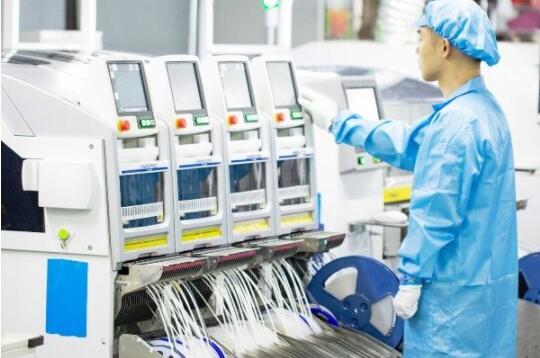
The people in the electronics industry involved in the PCB manufacturing process are very important. Printed circuit boards, printed circuit boards, are very widely used as the basis of electronic circuits. Printed circuit boards are used to provide a mechanical basis on which circuits can be built. So almost all printed circuit boards used in circuits and their designs are used in millions.
Although PCBs today form the basis of almost all electronic circuits, they are often taken for granted. However, the technology is advancing in this regard. Track size is reduced, the number of layers is increasing to accommodate the increased connectivity required, and design rules are improving to ensure that smaller SMT devices can be handled and the soldering process used in production can be accommodated.
The PCB manufacturing process can be implemented in various ways and has many variations. Despite many small changes, the main stages in the PCB manufacturing process are the same.
PCB composition

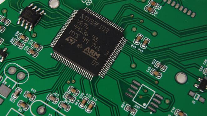
Printed circuit boards, printed circuit boards, can be made from a variety of different substances. The most widely used form of glass fiber substrate called FR4. This provides a reasonable degree of stability under temperature changes and is not as severe as breakdown, although not being overly expensive. Other less expensive materials can be used for printed circuit boards in low-cost commercial products. For high-performance RF designs, the dielectric constant of the substrate is important, and a low level of loss is required, and then PTFE-based printed circuit boards can be used, although they are more difficult to handle.
In order to make the tracks with the components in the PCB, first obtain the copper clad board. This includes both sides of the substrate material, usually FR4, and the usual copper cladding. The copper coating is connected to a thin layer of copper on the motherboard. This combination is usually very good for FR4, but the properties of PTFE make this more difficult, which increases the difficulty of PTFE PCB processing.
Basic PCB manufacturing process
With the bare PCB board selected and provided, the next step is to create the required tracks on the circuit board and remove the unwanted copper. The manufacturing of the PCB is usually achieved using a chemical etching process. The most common form of PCB etching used is ferric chloride.
In order to obtain the correct pattern of the track, the photographic process is used. Usually the copper of the bare printed circuit board is covered with a thin layer of photoresist. It then passes through a photographic film or photomask, specifying the required track exposure. In this way the image of the track is transferred to the photoresist. With this completed, the photoresist is placed in the developer so that only those areas of the track plate that are needed are covered in the resist.
The next stage in the process is to place the printed circuit board onto the iron chloride etched area where there is no need for tracks or copper. Knowing the concentration of ferric chloride and the thickness of copper on the circuit board, it is placed into the amount of time required to etch the bubble e-commerce. If the printed circuit board is placed in the etching for too long, then some definition is lost as ferric chloride will tend to weaken the photoresist.
Although most PCB boards are manufactured using photographic processing, other methods are also available. One is to use a specialized highly accurate milling machine. Then the machine is controlled to grind the copper far away in areas where it is not needed. The control is obviously automatic, driven from a file generated by the PCB design software. This form of PCB manufacturing is not suitable for large quantities, but it is an ideal choice in many situations where very small quantities of PCB prototypes are required.
Another method that is sometimes used on PCB prototypes is to print an etching resist ink on the printed circuit board using the screen printing process.