This article is mainly about the introduction of SMT chip processing technology and bad definition standards
The main SMT chip processing plant in the electronic processing industry, whether it is a one-stop service provider or a pure SMT chip manufacturer, SMT chip processing must consider the control of the process.
On the surface, the SMT process requires that the components are placed neatly, the components and the pads are centered, and the in-depth quality requirements need to be free of errors, omissions, reverse, virtual, and false soldering.
Specifically, the components corresponding to each pad have been determined at the beginning of the design. The components must correspond to the patch data of the Gerber data, and the specifications and models must be correct. The positive and negative components also affect the normality of the product. Whether or not, for example, the front and back of the silk screen layer determines whether the functional indicators of the design can be achieved. Especially (diodes, triodes, tantalum capacitors) these, positive and negative determine the realization of the function.
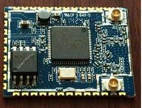
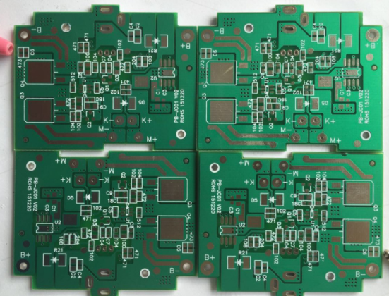
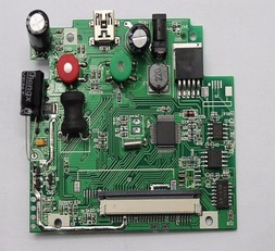
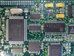
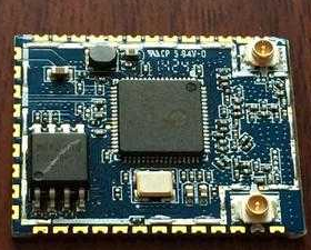
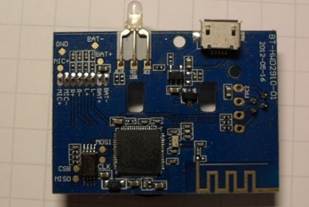
SMT chip processing

The multi-pin and complexity of BGA and IC components determine its very high requirements for quality. The solder joints are connected to tin and bridges. BGA soldering must be tested by X-RAY. In addition, the residual amount of tin beads and tin dross on the PCB pad also affects the quality of the product. Process control needs to be focused on.
At the quality summary meeting of SMT chip processing plants, we often hear words such as wrong, omission, reverse, false, and false soldering. Undoubtedly, the definition of bad items related to SMT chip processing is closely related to this. Get up and take a look!
1. Missing soldering: opening soldering, including soldering or separation of the pad and the substrate surface.
2. Wrong soldering: the material is not correctly loaded, and the part number of the component does not match the actual design material.
3. Welding: After welding, electrical isolation sometimes occurs between the welding end or the pin and the pad.
4. Tombstone: the tombstone, the soldering end of the component leaves the pad to stand upright or obliquely upward.
5. Shift: Inconsistent with the pad position during component mounting, cheap pad.
6. Trailing wire drawing: The solder has protruding burrs, is not connected to other conductors, or is connected incorrectly, which may cause short circuits and other reasons.
7. Reverse: The material is reversed, because more and more products nowadays are pursuing miniaturization and intelligence. Compared with the smaller and smaller materials, 01005/0201 components appear more and more, and anti-sticking often appears.
8. Less tin: Too little tin will cause the SMT solder joints to fall off easily and cause false soldering.
9. Residue: Compared with less tin, solder paste residue also needs attention. Excessive tin beads and tin dross residue will cause short-circuit and other quality problems under certain working conditions.