It does not meet the requirements of manufacturing capabilities, which requires a lot of maintenance work, resulting in low product quality and multiple revisions to product designs.
Products cannot be manufactured at all, designers must start from scratch, wasting a lot of manpower and material resources, and seriously weakening the competitiveness of enterprises in the same industry.
Poor product reliability, many customer complaints, large investment in after-sales service, companies cannot make ends meet, and the product life cycle is shortened, which ultimately leads to unsustainable companies.
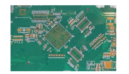
All kinds of problems are connected with the manufacturability of PCBA, which is an important factor that must be considered in the design of modern electronic products.
Guidelines for rework and repair (denso refurbishment, secondary soldering) in PCBA processing
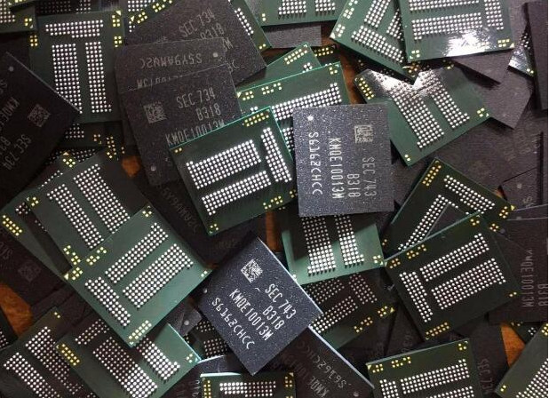
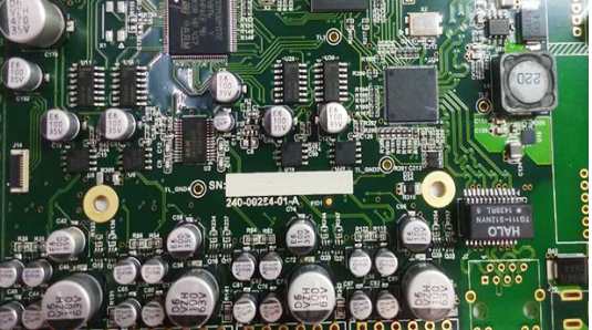
PCBA rework and repair

Rework and repair basis: Rework and repair do not have design documents and regulations, have not been approved in accordance with relevant regulations, and there is no specific rework and repair process regulations.
Permissible rework times for each solder joint: Rework is allowed for defective solder joints, and the rework times for each solder joint shall not exceed three times, otherwise the welding part will be damaged.
Use of dismantled components: In principle, dismantled components should not be used again. If they need to be used, they must be screened and tested according to the original electrical and technological performance of the components, and installation is allowed only when they meet the requirements.
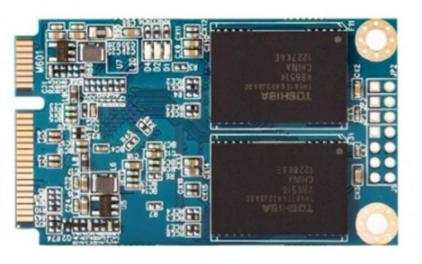
Number of unsoldering on each pad: Each printed pad should only be unsoldered once (that is, only one component is allowed to be replaced), and the thickness of the intermetallic compound (IMC) of a qualified solder joint is 1.5~3.5 µm, the thickness will increase after remelting, and even reach 50µm, the solder joints become brittle, the welding strength decreases, and there are serious reliability risks under vibration conditions; and the remelting IMC requires a higher temperature, otherwise the IMC cannot be removed. The copper-plated layer at the exit of the through hole is the thinnest, and the pad is easily broken from there after remelting; with the thermal expansion of the Z axis, the copper layer deforms, and the pad is separated due to the obstruction of the lead-tin solder joint. In the case of lead-free, the entire pad will be pulled up: PCB is delaminated after heating due to moisture in the glass fiber and epoxy resin: multiple soldering, the pad is easy to warp and separate from the substrate.
The bow and torsion requirements of surface mount and mixed mounting PCBA assembly and soldering: the bow and torsion requirements of surface mount and mixed mounting PCBA assembly and soldering are less than 0.75%
Total number of repairs of PCB assembly: The total number of repairs of one PCB assembly is limited to six, and excessive repairs and modifications affect reliability.