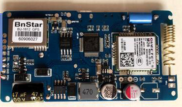
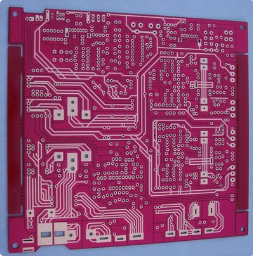
With the technological development of electronic products, circuits are becoming more and more dense, and the number of components on a single board is increasing, and the risk of damaged parts is correspondingly increased. In this article, it is explained in detail how to standardize the operation in the SMT process to avoid the occurrence of damaged parts.
Operational problems causing collisions
In-process damage-impact fracture, stress damage
1 Improper setting of thimble
The support in the immediate area is destroyed when the bending stress is applied to the placement or testing.
The damage feature of the resistor is fracture or electrode peeling, and the capacitor is in the inclined crack mode. If it is the first process part, the tombstone phenomenon of the fractured part may be seen after reflow.
2 stress damage
Poor board feeding causes deformation of the splint (card board) or manual bending of the board; poor suction nozzle and improper height setting can cause damage to the component.
The typical feature of damage is frontal rupture, and the rupture is usually separated after passing the furnace; if it is side damage, the chamfered slope is mostly cut off. Under this condition, the location of the impact point can be clearly distinguished.

Operational problems that cause collisions 2.
Damage after SMT process-impact rupture,
Stress damage, layer peeling (thermal shock)
1 impact rupture
Generally, it is difficult to determine the impact point in a lateral impact, because the PAD is usually peeled off (resistance) or the electrode of the part has broken (capacitance); while the impact point is easier to identify in the longitudinal impact part, and the PAD is generally not damaged, but the parts can see obvious defects. Horn.
2 stress damage
Damage caused by pressure and bending due to the folding of the edge of the plate, the test fixture, the placement of the trolley, etc. This type of damage usually appears in the form of an inclined crack.
3-layer peeling
SMT welding is caused by improper repair. Typical features are burnt black FLUX near the part, rough surface discoloration, layer peeling (capacitance), character surface peeling, etc.
How to start analyzing damaged parts
1 According to the point of impact analysis
The presence or absence of an impact point is not an absolute analysis and judgment factor, but usually the location, direction and damage degree of the impact point will provide a lot of analysis information.
a. The straight impact force usually causes damage to the PCB, and obvious damage defects can be seen on the components.
b. Parallel impact force will directly cause damage to the part due to rupture and missing corners, but because the direction of the torque is not large, it will not cause serious damage to the PAD most of the time.
2According to the crack shape
a. Delamination cracks: Most of the causes of delamination are due to thermal shock, but part of the reason is poor SMT component manufacturing process, because the layer-to-layer bonding and Baking process defects cause delamination after reflow.
b. Oblique cracks: due to the bending stress forming a fulcrum at the lower part of the part, the fixed solder joints produce the oblique surface phenomenon of fracture at the electrode end, especially the large-size components perpendicular to the stress direction are most severely broken.
c. Radial cracks: Radial cracks generally have impact points to follow, mostly caused by point pressure, such as thimble, suction nozzle, test fixture, etc.
d. Complete rupture: Complete rupture is the most serious failure mode, and it is often accompanied by PCB damage. It is usually caused by lateral impact or capacitor cracks causing the device to burn out.
3 According to the displacement of the parts
When the part has longitudinal cracks or the reflow is heated but not broken, it is very likely that only the cracks are seen but there is no separation, which will cause inspection troubles. The cracks that have been caused before the reflow will be pulled apart due to the tensile force of the melting of the solder, and there will be tombstones on the fractured parts even during the back process. Most of the causes are damage to the components in the first process, bending stress, or improper setting of the ejector pins in the second process. Of course, cracks caused by cutting and packaging in the component manufacturing process may also be broken by heat after reflow.
The source of the problem in production and
solution
1 Warehouse storage
Problem 1: The incoming material is bad, and the incoming packaging method is unreasonable.
Solution: Ask the supplier to improve the packaging method.
Question 2: The temperature and humidity of the warehouse are not up to standard.
Solution: The warehouse manager regularly checks the thermometer and hygrometer to see if it is within the specification range.
Question 3: The storage and packaging method is unreasonable.
Solution: Strict and professional storage and stacking methods prevent the packaging method from deforming, creeping and damaging parts.
2 Material preparation room
Question 1: In the process of transferring materials from the warehouse, parts may be damaged due to falling and impact.
Solution: Add a protective railing to the material rack.
Question 2: When the packaging method is changed, the parts are damaged due to the incorrect action method.
Solution: Standardize operation.
Question 3: The vacuum packaging of moisture-sensitive parts is damaged, causing air leakage, etc.
Solution: go online after baking or vacuum packaging after baking, etc.
3SMT production line picking
Question 1: In the process of transferring materials from the preparation room, there may be damage to parts such as falling and impact.
Solution: Add protective railings, etc. to the material rack.
Problem 2: In the process of receiving materials or cutting materials, the parts are damaged.
Solution: Use the correct methods and tools.
4 into the board
Problem: The PCB board is bent and deformed when it enters the Magazine non-parallelly.
Solution: When installing the board, install the board in parallel to avoid collision between the PCB and Magazine.
5GKG printing, CP placement
Problem: The top Pin setting in the machine is wrong, which causes the back welding to be knocked out.
Solution:
1. The top pin map created by the operator can only be used after confirmation by ME.
2. IPQA check whether the top pin is in line with the top pin diagram before opening the line
6 CP&QP components
Question 1: The height setting in Part data is smaller than the height of the part body, and the part is crushed when the part is placed.
Solution: The height of Part data should be greater than or equal to the height of the part body.
Question 2: The top Pin height is abnormal.
Solution: unify the height of the top pin. It needs to be measured after adjustment.
7Reflow
Problem: When the LOADER in front of the AOI is full, or the track emergency switch is pressed, or the track sensor fails, the front plate does not flow down after the reflow oven is discharged, and the board that passes through the reflow oven continues to flow down, causing the back board to hit the front plate .
Solution:
1. Improve the detection speed of AOI;
2. The SMT production line arranges personnel near this station to pay attention to the buzzer alarm and ensure that the board is taken out before the collision.