Causes and control methods of voids formed in SMT welding
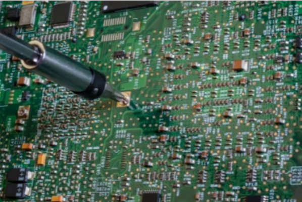
In SMT patch processing, welding is a highly demanding process, which is prone to various small problems. If it cannot be solved properly, it will also affect product quality. Take welding porosity as an example. This is a problem related to welded joints. The existence of porosity will affect the mechanical properties of welded joints. This is because the growth of pores will evolve into large cracks, increase the burden on the solder, and damage the joints. Strength, ductility and service life. So what is the reason for the porosity formed by SMT welding? How to control the reduction? The following is an introduction for everyone.
The reason for the porosity formed by SMT patch welding:
During the welding process, the mechanism for forming pores is more complicated. Normally, the porosity is caused by the flux degassing entrained in the solder in the sandwich structure during reflow (2,13). The formation of pores is mainly determined by the solderability of the metallized area, and changes with the decrease of flux activity, the increase of the metal load of the powder, and the increase of the coverage area under the lead joint. Reducing the size of the solder particles can only increase by a margin. Pores.
In addition, the formation of pores is also related to the time allocation between the coalescence of solder powder and the elimination of fixed metal oxides.

The earlier the solder paste coalesces, the more voids are formed. In addition, the solder shrinks when it solidifies, and the delamination of exhaust gas and the entrained flux when soldering plated through holes are also the reasons for the porosity.
2. Methods of controlling the formation of pores in SMT patches:
1. Use a flux with higher activity;
2, improve the solderability of components or PCB circuit boards;
3. Reduce the formation of powdered oxides in solder;
4. Adopt inert heating atmosphere;
5. Reduce the preheating degree of reflow lead.
Classification characteristics of welding materials in SMT patch processing
According to its components, solder in SMT chip processing can be divided into tin-lead solder, silver solder, and copper solder. According to the environmental humidity used, it can be divided into high temperature solder (solder used under high temperature) and low temperature solder (solder used under low temperature environment). In order to ensure the quality of soldering during patch processing, it is important to choose different solders depending on the object to be soldered. In the assembly of electronic products, tin-lead series solders, also called solders, are generally used.
Tin has the following characteristics:
1. Good conductivity: Because tin and lead solder are good conductors, its resistance is very small.
2. Strong adhesion to component leads and other wires, not easy to fall off.
3. Low melting point: it can be melted at 180 degree Celsius, and it can be welded with 25W external heating type or 20W internal heating type electric soldering iron.
4. It has certain mechanical strength: because the strength of tin-lead alloy is higher than that of pure tin and pure lead. In addition, due to the light weight of the electronic components, the strength requirements of the solder joints in the SMT patch are not very high, so the strength requirements of the solder joints can be met.
5. Good corrosion resistance: The welded PCB circuit board can resist atmospheric corrosion without applying any protective layer, thereby reducing the process flow and reducing the cost.
Among tin-lead solders, those with a melting point below 450°C are called soft solders. Anti-oxidation solder is the solder used in automated production lines in industrial production, such as wave soldering. When this liquid solder is exposed to the atmosphere, the solder is extremely easy to oxidize, which will cause false soldering, which will affect the quality of soldering. Therefore, adding a small amount of active metal to the tin-lead solder can form a covering layer to protect the solder from further oxidation, thereby improving the soldering quality.
Because tin-lead solder is composed of two or more metals in different proportions. Therefore, the properties of tin-lead alloys will change as the ratio of tin-lead changes. Due to different manufacturers, the configuration ratio of tin-lead solder is very different. In order to make the solder ratio meet the needs of soldering, it is important to choose a suitable ratio of tin-lead solder.
The commonly used solder matching ratios are as follows:
1. Tin 60%, lead 40%, melting point 182 degree Celsius;
2. Tin 50%, lead 32%, cadmium 18%, melting point 150 degree Celsius;
3. Tin 55%, lead 42%, bismuth 23%, melting point 150 degree Celsius.
There are several shapes of PCB solder, such as wafer, ribbon, ball, and solder wire. The commonly used solder wire contains solid flux rosin inside. There are many types of solder wire diameter, commonly used 4mm, 3mm, 2mm, 1.5mm and so on.