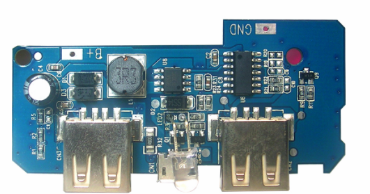
Environmental conditions for storage of SMT components:
Ambient temperature: inventory temperature <40 degree Celsius.
The temperature at the production site is less than 30°C.
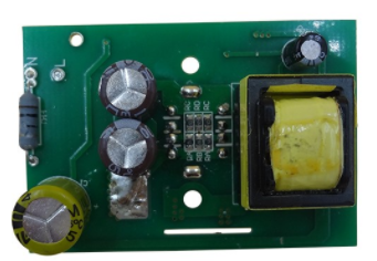
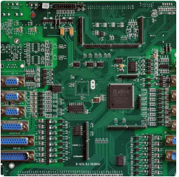
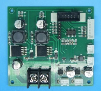
Environmental humidity: Ambient atmosphere: There must be no sulfur, chlorine, acid and other toxic gases that affect welding performance in the inventory and use environment. Anti-static measures: to meet the anti-static requirements of SMT components. Component storage period: Calculated from the production date of the component manufacturer, the inventory time should not exceed 2 years; the inventory time after purchase by the user of the complete machine factory generally does not exceed one year; if it is a complete machine factory with a relatively humid natural environment, purchase SMT components should be used within 3 months after being imported, and appropriate moisture-proof measures should be taken in the storage place and component packaging. SMD devices with moisture-proof requirements. It must be used up within 72 hours after opening, and the longest should not exceed one week. If it can't be used up, it should be stored in a RH20% drying box. SMD devices that have been damp should be dried and dehumidified according to regulations. For SMD (SOP, Sj, lCC, QFP, etc.) packed in plastic tubes, the packaging tube is not resistant to high temperatures and cannot be directly put in the oven for baking. It should be placed in a metal tube or metal tray for baking. QFP's packaging plastic tray has two types: non-high temperature resistant and high temperature resistant. High temperature resistant (with Tmax=135°C, 150°C or max180°C, etc.) can be directly put into the oven for baking; those that are not resistant to high temperature can not be directly put into the oven to bake to prevent accidents and should be placed separately Bake in a metal pan. Avoid damaging the pins when transferring, so as not to destroy its coplanarity. SMT components Transportation, material separation, inspection or manual placement: If workers need to take SMD devices, they should wear an anti-static wrist strap, try to use a suction pen to operate, and pay special attention to avoid bumping the pins of SOP, QFP and other devices to prevent pin warping. Use the original intact packaging bag. As long as the bag is not damaged and the desiccant inside is good (all the black circles on the humidity indicator card are blue and no pink), the unused SMD can still be repacked into the bag, and then sealed with tape. What to pay attention to when designing PCBA circuit board Circuit design 1. For standard components, attention should be paid to the dimensional tolerances of components from different manufacturers. For non-standard components, the pad pattern and pad spacing must be designed according to the actual size of the component. 2. When designing a high-reliability circuit, the pad should be widened, and the pad width=1.1~1.2 times the width of the solder end of the component. 3. When designing high-density PCBA, the pad size of the components in the software library should be corrected. 4. The distance between various components, wires, test points, through holes, pad and wire connection, solder mask, etc. must be designed according to different processes. 5. Consider repairability. 6. Consider issues such as heat dissipation, high frequency, and anti-electromagnetic interference. 7. The placement and direction of the components should be designed according to the requirements of the reflow soldering or wave soldering process. For example, when using the reflow soldering process, the placement direction of the components should consider the direction the printed circuit board enters the reflow soldering furnace. When adopted. ; During wave soldering, PLCC, FP, connectors and large-size SOIC components cannot be placed on the wave soldering surface; in order to reduce the wave shadow effect and improve soldering quality, there are special requirements for the placement direction and position of various components; When designing wave soldering pad patterns, the pad lengths of rectangular components, SOT and SOP components should be extended, and the two outermost pairs of SOP pads should be widened to absorb excess solder, less than 3.2mm *1.6mm rectangular components can be chamfered at both ends of the pad with 45°, and so on. 8. The design of the printed circuit board should also consider the equipment. Different placement machines have different mechanical structures, alignment methods, and printed circuit board transmission methods. Therefore, the position of the positioning hole of the printed circuit board, the figure and position of the reference mark (Mark), the edge shape of the printed circuit board, and the printed circuit board are different. There are different requirements for the positions where the components cannot be placed near the side of the circuit board. If the wave soldering process is used, the process margins that need to be left in the printed circuit board transmission chain should also be considered.