Mixed tools
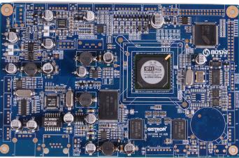
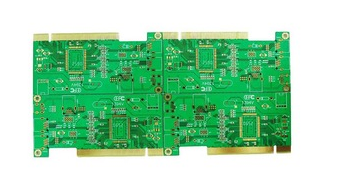
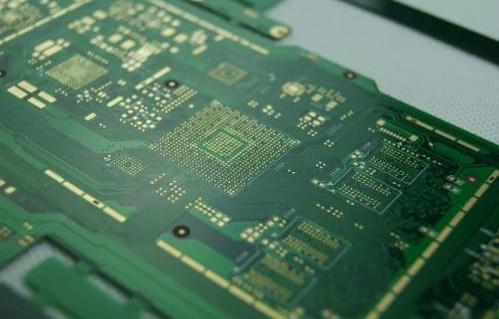
The characteristics of the mixed assembly process are: on one side of the PCB circuit board (the A side has a different number of IC components, and through-hole components are inserted, and there are many chip resistors on the other side of the PCB (side B) Electrical components (and sometimes ICs) are often called "mixed packages." They retain the advantages of low-cost through-hole components, and are common in audio-visual products, such as CDs and DVDs.
The mixing process operation process is: soldering IC components with solder paste-reflow soldering process on the A side; coating the patch glue on the B side and sending it to the infrared oven for curing; then transfer to the A side and insert the through-hole components ; Wave soldering side B; PCB finishing, cleaning, testing, and assembly.
The ultimate purpose of bonding SMD/SMC on the PCB is to solder, but only bonding the components to the PCB (excluding all bonding defects) does not guarantee that the SMA can be soldered well through wave soldering. This is because of the chip components. There are almost no leads, and SMC/SMD has its particularity in wave soldering.
During wave soldering of through-hole components, the lead of the component is in contact with the high-temperature solder wave and under the action of the flux, the wetting force promotes the solder to extend the lead to climb up, so as to wet the entire pad to obtain a good soldering effect. If the hole on the PCB is a metal hole, the solder can extend through the metal hole to the other side of the PCB and form a full solder joint.

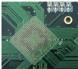
However, chip devices have no pins and are directly bonded to the PCB. The components and the PCB surface form an acute angle, so that the flowing solder wave impacts the surfaces of the resistors and capacitors in the tangential direction, and it is not easy to reach the rectangular components and the PCB plane. The corners are more obvious as the original thickness increases. In this corner, bubbles and flux residues formed by the flux tend to accumulate, resulting in missed soldering or poor soldering. People often refer to this corner as the "welding dead zone".
Another problem of SMT-wave soldering is that the soldering heads of chip components are usually coated with SnPb, which has good solderability. In order to ensure the flatness of the PCB, the surface is usually coated with gold plating or preheated flux. The soldering effect is not as good as the SnPb alloy hot air leveling process. When passing through the solder wave, the wetting time of the two is different. Usually, the SnPb terminal electrode is only 0.1s, and the copper layer takes 0.5s. The end of the component first contacts the solder, so it is easy to cause "welding dead zone". In order to solve the defect of "welding dead zone", dual-wave soldering technology is usually used, that is, increasing the pulse wave to make the solder wave impact the "welding dead zone" in the vertical direction to achieve a good welding effect.
In addition, low solid content flux should be used to reduce the residue in the dead zone; increase the PCB preheating temperature to improve solderability; improve the arrangement of components and reduce the dead zone corners to reduce the rate of bad solder joints.
Therefore, the wave soldering of SMC/SMD components should be strictly checked. The arrangement direction of the components should be considered during PCB design, and the direction of the component pins should be perpendicular to the direction of movement during wave soldering as much as possible. IC components should be as close as possible. Place the ground on the A side of the PCB, less on the B side, and the IC components that must be placed on the B side. Not only the arrangement direction, but also the auxiliary pads should be added. The activity and density of the flux are also requirements that cannot be ignored. In addition, the curing strength of the components should meet the requirements, especially the residual glue should not be adhered to the pad.