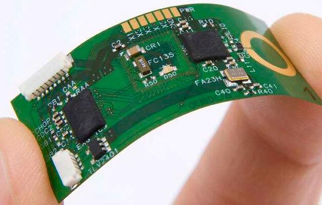
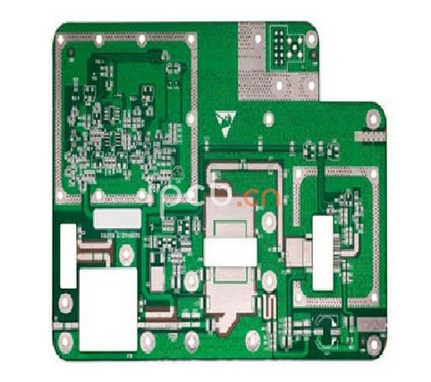
SMB design
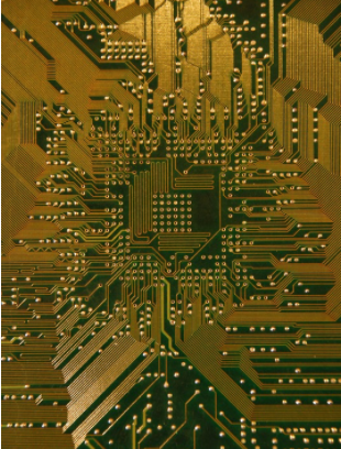
1. Component layout
The layout is to arrange the components evenly and neatly on the PCB in accordance with the requirements of the electrical schematic diagram and the dimensions of the components, and can meet the mechanical and electrical performance requirements of the whole machine. Whether the layout is reasonable or not not only affects the performance and reliability of the PCB assembly and the whole machine, but also affects the difficulty of PCB and its assembly processing and maintenance, so try to do the following when layout:
The components are evenly distributed, and the components of the same unit circuit should be arranged relatively concentratedly to facilitate debugging and maintenance;
Components with interconnections should be arranged relatively close to each other in order to increase the wiring density and ensure the shortest wiring distance;
Components that are sensitive to heat should be arranged far away from components that generate large amounts of heat;
The components that may have electromagnetic interference with each other should be shielded or isolated.
2. Wiring rules
Wiring is to lay out printed wires in accordance with the electrical schematic diagram, wire table, and the required wire width and spacing. The wiring should generally comply with the following rules:
Under the premise of meeting the requirements of use, the wiring can be simple and not complicated, and the order of the wiring method is single layer, double layer-multilayer.
The wire layout between the two connecting plates should be as short as possible, and sensitive signals and small signals should go first to reduce the delay and interference of small signals. Ground wire shielding should be laid next to the input line of the analog circuit; the wiring of the same layer should be evenly distributed; the conductive area on each layer should be relatively balanced to prevent the board from warping.
When changing the direction of the signal line, it should be oblique or smooth, and the radius of curvature should be larger to avoid electric field concentration, signal reflection and additional impedance.

The wiring of the digital circuit and the analog circuit should be separated to avoid mutual interference. If they are on the same layer, the wires of the ground system and the power system of the two circuits should be laid separately, and the signal wires of different frequencies should be separated by laying ground wires., To avoid crosstalk. For the convenience of testing, necessary breakpoints and test points should be set in the design.
When circuit components are grounded and connected to power, the traces should be as short as possible and as close as possible to reduce internal resistance.
The upper and lower layer traces should be perpendicular to each other to reduce coupling, and the upper and lower traces should not be aligned or parallel.
The lengths of multiple I/O lines of high-speed circuits and the IO lines of circuits such as differential amplifiers and balanced amplifiers should be equal to avoid unnecessary delay or phase shift.
When the pad is connected to a larger conductive area, a thin wire with a length of not less than 0.5mm should be used for thermal isolation, and the width of the thin wire should not be less than 0.13mm.
The wire closest to the edge of the board should be more than 5mm away from the edge of the printed board, and the grounding wire can be close to the edge of the board when needed. If the guide rail is to be inserted during the processing of the printed board, the distance between the wire and the edge of the board must be at least greater than the depth of the guide groove.
The common power and ground wires on the double-sided board should be routed as close to the edge of the board as possible and distributed on the surface of the board. The multi-layer board can be provided with a power layer and a ground layer on the inner layer, and connect to the power and ground wires of each layer through metallized holes. Bonding force between layers of multi-layer boards.
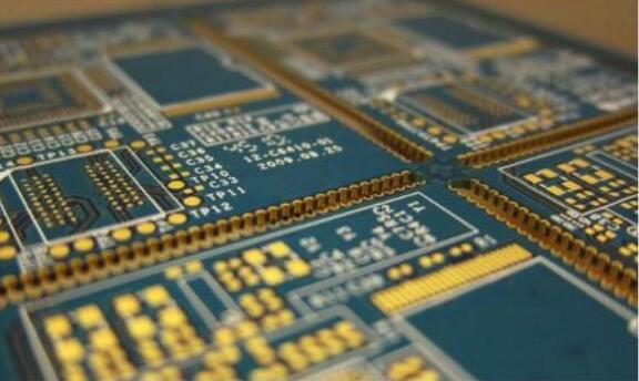
3. Wire width
The width of the printed wire is determined by the load current of the wire, the allowable temperature rise and the adhesion of the copper foil. Generally, the wire width of the printed board is not less than 0.2mm, and the thickness is more than 18μm. The thinner the wire, the more difficult it is to process. Therefore, when the wiring space allows, a wider wire should be selected appropriately. The general design principles are as follows:
The thickness of the signal line should be the same, which is beneficial to impedance matching. Generally, the recommended line width is 0.2~0.3mm (812mil). For the power ground line, the larger the wiring area, the better to reduce interference. It is best to shield the high-frequency signal with a ground wire, which can improve the transmission effect.
In high-speed circuits and microwave circuits, the characteristic impedance of the transmission line is specified. At this time, the width and thickness of the wire should meet the characteristic impedance requirements.
In the design of high-power circuits, the power density should also be considered. At this time, the line width, thickness, and insulation performance between lines should be considered. If it is an inner conductor, the allowable current density is about half of that of the outer conductor.
4. Printed wire spacing
The insulation resistance between the conductors on the surface of the printed board is determined by the spacing of the conductors, the length of the parallel sections of adjacent conductors, and the insulating medium (including the base material and air). When the wiring space allows, the spacing of the conductors should be appropriately increased.
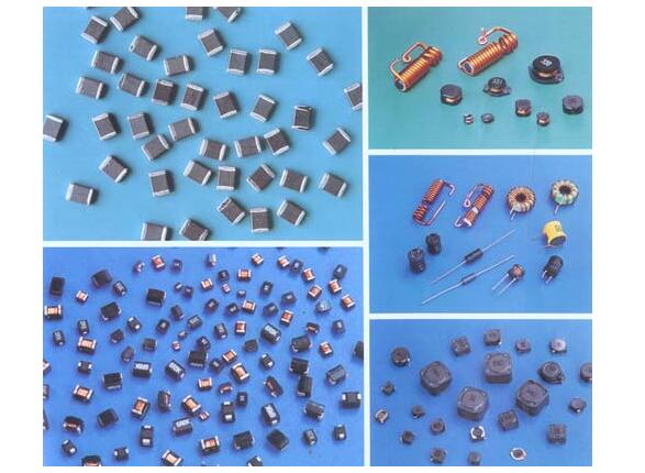
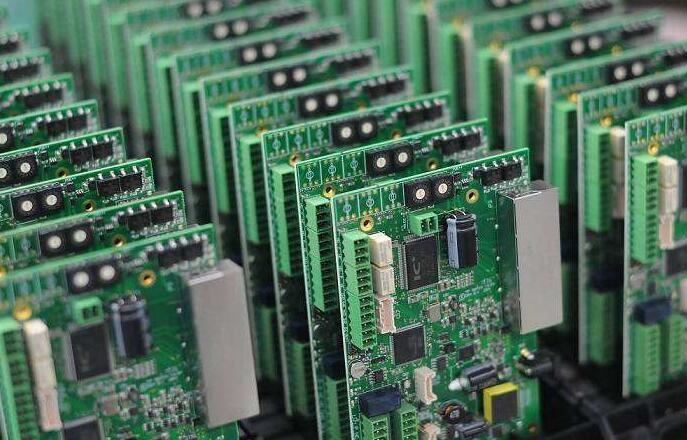
5. Selection of components
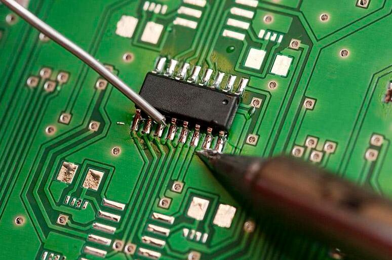
The selection of components should fully consider the actual area of the PCB board, and use conventional components as much as possible. Don't blindly pursue small-size components to avoid increasing costs. IC devices should pay attention to the pin shape and pin spacing. QFPs with a pin spacing of less than 0.5mm should be carefully considered. It is better to directly choose BGA packaged devices. In addition, the packaging form of the components, terminal electrode size, solderability, device reliability, temperature tolerance (such as whether it can meet the needs of lead-free soldering) should be considered.
After selecting the components, a database of components must be established, including relevant information such as installation dimensions, pin dimensions, and manufacturers.
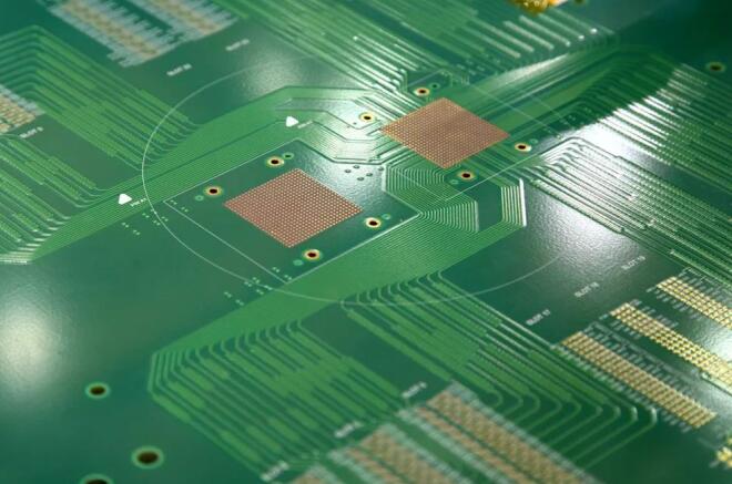
6. Selection of PCB substrate
The substrate should be selected according to the use conditions and mechanical and electrical performance requirements of the PCB; the number of copper-clad surfaces of the substrate (single-sided, double-sided or multi-layer board) should be determined according to the printed board structure; according to the size of the printed board, The unit area carries the mass of the components and determines the thickness of the substrate board. The cost of different types of materials varies greatly. The following factors should be considered when choosing a PCB substrate
Electrical performance requirements;
Factors such as Tg, CTE, flatness and the ability of hole metallization;
The price factor.