PCBA processing has many factors that affect bridging, such as design, flux activity, solder composition, process, etc., which require continuous improvement in many aspects.
According to the causes, bridging can be roughly divided into two types: insufficient flux type and vertical layout type.
(1) Insufficient flux type.
The characteristic is that there is no wetting or partial wetting of multi-leads with tin, pads, and lead heads (the most prone to oxidizing gas).
(2) Vertical layout type.
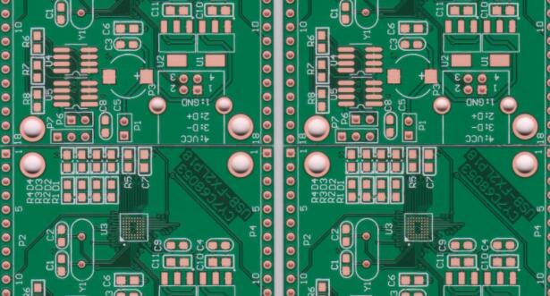
The characteristics are full solder joints, tin-coated lead heads, and tin-connected suspension. This is a common type of bridging. As its classification name, it is mainly related to the layout of the components on the PCB, followed by the size of the pad, the lead spacing, and the thickness of the lead., Lead wire extension length, flux activity, tin wave height, preheating temperature and chain speed are related. There are many influencing factors and complex factors, which are complicated and difficult to solve 100%. Generally, it occurs in connector components with relatively small lead spacing (≤2mm), relatively long extension (≥1.5mm), and relatively thick.
improvement measures:

A) Design
(1) The most effective measure is to use short lead design
For 2.5mm pitch leads, the length should be controlled within 1.2mm; for 2mm pitch leads, the length should be controlled within 0.5mm. The simplest experience is the "1/3 principle", that is, the lead length should be 1/3 of its pitch. As long as this is done, the bridging phenomenon can basically be eliminated.
(2) Components such as connectors
As far as possible, the length direction of the components should be arranged parallel to the transmission direction and the soldering process pads should be designed to provide continuous carrier capability. When welding, the direction can be turned 90° to make it parallel to the transmission direction.
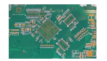
(3) Use small pad design
Because the strength of the PCB solder joints of the metallized holes basically does not depend on the size of the pads. In terms of reducing bridging defects, the smaller the width of the pad ring, the better, and the minimum ring width that mainly meets the needs of PCB manufacturing.
Two) Process
(1) Use a narrow flat wave soldering machine for soldering
(2) Use an appropriate transmission speed (it is advisable that the lead wire can be detached continuously)
Fast or slow chain speed is not conducive to the reduction of bridging phenomenon. This is because (traditional explanation) the chain speed is fast, and the time to open the bridge is not enough or the heating is insufficient; the slow chain speed may cause the temperature of the lead near the package end to drop. But the actual situation is far more complicated than this. Sometimes, a lead with a large heat capacity and a long lead should be fast, and vice versa.
The standard for judging the speed of the chain depends on the welding object and the equipment used. It is a dynamic concept, usually 0.8~1.2mm/min as the demarcation point.
(3) The preheating temperature should be appropriate and the flux should reach a certain viscosity. If the viscosity is too low, it will be easily washed away by the solder wave and will make the wetting worse. Excessive preheating will cause the rosin to oxidize and polymerize, slowing down the wetting process. This will increase the probability of bridging.
(4) The bridging caused by non-flux can be eliminated by reducing the wave height.
(5) Use lead-free solder alloys with low viscosity, such as NIHON SUPERIOR's SN100C (Sn-Cu-Ni-Ge, with a melting point of 227°C), which is a kind of no bridge, no shrinkage, and the most successful solder alloy in the industry. Silver lead-free PCBA solder.