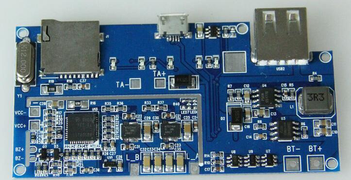
In the PCBA processing process, non-contact printing uses a flexible screen template to print, and a necessary gap is set between the template and the PCB. The following SMT production technicians will tell you what is the principle and process of non-contact printing.
Before printing, place the PCB on the working support, use suspension or mechanical fixation, and tighten the screen with the printed graphic window on a metal frame and align it with the PCB. There is a necessary distance between the top of the PCB and the bottom of the screen (usually called a scratch gap). At the beginning of printing, put the solder paste on the screen in advance, and move the squeegee from one end of the screen to the other end, and press the screen to make it contact with the PCB surface, and at the same time press the solder paste to make it pass through the graphic window on the screen. Deposited on the PCB pads.
Solder paste and other printing pastes are a kind of fluid, and the printing process follows the principles of fluid mechanics. Screen printing has the following three characteristics:

The solder paste in front of the squeegee rolls along the advancing direction of the auxiliary blade; the screen is separated from the PCB surface by a short distance; the solder paste is transferred from the mesh to the PCB surface during the process of the screen from contact to the PCB surface.
When in use, the stroke of the print head must be set so that it exceeds a certain distance from the edge of the graphic, otherwise a too small stroke will deform or irregular the printing of the edge. If the pressure of the print head is too small, the solder paste cannot reach the bottom of the template opening effectively, and it cannot be deposited on the pads well. It may also prevent the screen from touching the PCB and affect the printing; the printing pressure is too high It will deform the auxiliary knife, and even take part of the solder paste in the larger openings on the template, forming a concave surface solder paste deposit, which will damage the template in severe cases. The method to choose the right strength is: first use the necessary pressure to obtain a uniform and thin layer of solder paste on the template, and then slowly increase the pressure so that every time it is printed, all the solder paste on the template is evenly scraped off. until.
In non-contact printing, when the secondary knife is separated from the PCB through the template, the solder paste is leaked onto the PCB pads, and printing is adopted in an extremely simple structure. However, with the increase in mounting density requirements and the generation of fine-pitch printing requirements, the problems of non-contact printing methods have become apparent.
The following lists several problems of non-contact printing in fine pitch solder printing.
(1) The printing position is deviated. Since the contact printing will deform the template, the solder paste on the template cannot be missed directly below, resulting in a deviation of the solder paste position.
(2) Insufficient filling amount, occurrence of deficiency. From a microscopic point of view, the shape of the opening is also changing as the template is deformed, which is the reason for the decrease in filling volume and the occurrence of weld shortage.
(3) Occurrence of penetration and bridging. Because there is a gap between the template and the PCB circuit board, the proportion of flux penetrating into this gap will increase. In extreme cases, the exudation of solder paste particles will cause bridging.