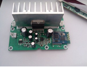
Factors affecting PCBA processing and cleaning
In the PCBA patch processing plant, in order to make the cleaning of printed circuit components proceed smoothly and achieve excellent results, it is necessary not only to be familiar with the cleaning mechanism, cleaning agent and cleaning method, but also to be familiar with the main factors that affect the cleaning effect, such as yuan Device type and arrangement, PCB design, flux type, welding process parameters, residence time after welding and solvent spray parameters, etc.
1. PCB design
During PCB design, it is necessary to avoid setting plated through holes under the components. In the case of wave soldering, the flux will flow to the upper surface of the SMA or under the SMD on the upper surface of the SMA through the plated through holes arranged under the components, which will cause difficulty in cleaning. The thickness and width of the PCB should match each other, and the thickness should be close. When selecting wave soldering, thinner substrates must be reinforced with ribs or plates to increase the resistance to deformation, and this reinforced structure will block the flux and is difficult to remove during cleaning. The welding mask should be able to maintain excellent adhesion, and there should be no microcracks or wrinkles after several welding processes.
2. Component type and arrangement

With the development of miniaturization and thinning of components, the distance between the components and the PCB is getting smaller and smaller, which makes it more and more difficult to remove the residue of the agent from the SMA. For example, complex components such as SOIC, OFP and PLCC will prevent the penetration and replacement of code cleaning solvents when cleaning after welding. When the surface area of the SMD increases and the lead center spacing decreases, especially when there are leads on all four sides of the SMD, the post-weld cleaning operation becomes more difficult. The arrangement of components affects the cleanability of SMA in two aspects: the direction of component lead extension and the orientation of components. They have a great influence on the flow speed, uniformity and flow of the cleaning solvent passing under the components.
3. Flux type
The type of flux is the main factor that affects the cleaning of SMA after welding. As the percentage of solids in the flux and flux activity increase, it becomes more difficult to clean the flux residue. For a specific SMA, which type of flux should be selected for welding, it must be considered in combination with the cleanliness level required by the component and the cleaning process that can meet this level.
4. Reflow welding process and residence time after welding
The effect of reflow welding process on cleaning is mainly manifested in the temperature and residence time of preheating and reflow heating, which is the rationality of the reflow heating curve. If the reflow heating curve is unreasonable, overheating of the SMA will cause the flux to deteriorate and it will be difficult to clean the deteriorated flux. The residence time after welding refers to the residence time before the components enter the cleaning process after welding, that is, the process residence time. During this time, the flux residue will gradually harden and cannot be cleaned off. Therefore, the residence time after welding should be as short as possible. For a specific SMA, the maximum allowable residence time must be determined according to the manufacturing process and the type of flux.
5. Spray pressure and speed
In order to better improve the cleaning efficiency and cleaning quality, in the choice of static solvent or steam cleaning, spray scouring is mostly used. The use of high-density solvents and high-speed spraying can make the pollutant particles subject to large forces and easy to be cleaned. But when the solvent is selected, the density of the solvent is no longer a parameter that can be circled, and the only adjustable parameter is the spray speed of the solvent.
PCBA generation processing requirements
One, the bill of materials
The components should be inserted or mounted in strict accordance with the bill of materials, PCB silk screen and outsourcing processing requirements. When the material does not meet the bill of materials, the PCB silk screen, or the process requirements are different, or the requirements are ambiguous and cannot be operated, it should be Contact our company immediately to confirm the accuracy of materials and process requirements.
2. Anti-static requirements
1. All components are treated as electrostatic sensitive devices.
2. All personnel who come into contact with components and products wear anti-static clothes, anti-static bracelets, and anti-static shoes.
3. During the raw materials entering the factory and in the warehouse, the electrostatic sensitive devices are all selected in anti-static packaging.
4. During operation, use anti-static work surface, and store components and semi-finished products in anti-static containers.
5. The welding equipment is grounded reliably, and the electric soldering iron is of anti-static type. All must pass the inspection before adopting.
6. The semi-finished PCB board is stored and transported in an anti-static box, and the isolation material is made of anti-static pearl cotton.
7. The whole machine without shell adopts anti-static packaging bag.
Third, the provisions of the component appearance mark insertion direction
1. Polarity components are inserted according to polarity.
2. For components with silk-screened on the side (such as high-voltage ceramic capacitors), when inserted vertically, the silk screen faces right; when inserted horizontally, the silk screen faces down. When the components (not including the chip resistors) silk-printed on the top are inserted horizontally, the font direction is the same as the direction of the PCB screen printing; when inserted vertically, the upper side of the font faces right.
3. When the resistance is inserted horizontally, the error color ring faces to the right; when the resistance is inserted vertically, the error color ring faces down; when the resistance is inserted vertically, the error color ring faces the board.
Four, welding requirements
1. The pin height of the plug-in component on the soldering surface is 1.5~2.0mm. SMD components should be flat against the board surface, and the solder joints should be smooth, without burrs, and slightly arc-shaped. The solder should exceed 2/3 of the height of the solder end, but should not exceed the height of the solder end. Low tin, spherical solder joints or solder covered patches are all unqualified products;
2. The height of the solder joints: the height of the solder climbing pins is not less than 1mm for the single-sided board, and the double-sided board is not less than 0.5mm and requires tin penetration.
3. Solder joint shape: Conical shape and covering the entire pad.
4. The surface of the solder joints: smooth, bright, no black spots, flux and other debris, no spikes, pits, pores, copper exposed and other defects.
5. Solder joint strength: fully wetted with pads and pins, no false soldering or false soldering.
6. Solder joint cross-section: the component's cutting foot should not be cut to the solder part as much as possible, and there should be no cracking on the contact surface between the lead and the solder. There are no spikes or barbs at the cross section.
7. Welding of the needle base: The needle base must be mounted on the bottom of the board, and the position should be in the correct direction. After the needle base is welded, the bottom of the needle base should not float.
Over 0.5mm, the skew of the seat body does not exceed the silk screen frame. Rows of needle holders should also be kept neat and not allowed to be misaligned or uneven.
Five, transportation
In order to prevent damage to the PCBA, the following packaging should be used during transportation:
1. Storage container: anti-static turnover box.
2. Isolation material: anti-static pearl cotton.
3. Placement spacing: there is a distance greater than 10mm between the PCB board and the board, and between the PCB board and the box.
4. Placement height: There is a space greater than 50mm from the top surface of the turnover box to ensure that the turnover box is not pressed against the power supply, especially the power supply of the wire.
Six, plate washing requirements
The board surface should be clean and free of tin beads, component pins, and stains. Especially at the solder joints on the plug-in surface, there should not be any dirt left by soldering. The following devices should be protected when washing the board: wires, connecting terminals, relays, switches, polyester capacitors and other easily corrosive devices, and the relays are strictly prohibited to be cleaned by ultrasonic.
Seven, all components are not allowed to go beyond the edge of the PCB board after the installation is completed.
8. When the PCBA is over the furnace, because the pins of the plug-in components are scoured by the tin flow, some plug-in components will be tilted after being soldered through the furnace, causing the component body to exceed the silk screen frame. Therefore, the repair soldering personnel after the tin furnace are required to properly perform it. Fix.