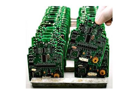
After PCBA production is completed, PCBA needs to be transported to customers in various ways. During the transportation process, the following requirements need to be paid attention to.
1. Packaging materials
PCBA board is a relatively fragile and easily damaged product. Before transportation, it must be carefully packaged in bubble bags, pearl cotton, electrostatic bags, and vacuum bags.
2. Anti-static packaging
Static electricity will penetrate the chips in the PCBA board. Because static electricity is invisible, intangible, and easy to generate, it is necessary to use anti-static packaging during packaging and transportation.
3. Moisture-proof packaging
Before packaging, the PCBA should be cleaned and dried on the surface, and sprayed with three-proof paint.
4. Anti-vibration packaging
Put the packaged PCBA board into an anti-static packaging box. When it is placed vertically, it should not be stacked up to more than two layers, and a spacer should be placed in the middle to keep it stable and prevent shaking.

The main points of PCBA process control and quality control
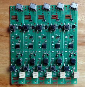
The PCBA manufacturing process involves many links. The quality of each link must be controlled to produce a good product. The general PCBA is made up of: PCB circuit board manufacturing, component procurement and inspection, SMT patch processing, plug-in processing, A series of processes such as program firing, testing, and aging.
PCBA process control
1. PCB circuit board manufacturing
After receiving the PCBA order, analyze the Gerber file, pay attention to the relationship between the PCB hole spacing and the board's load-bearing capacity, do not cause bending or breakage, and whether the wiring considers key factors such as high-frequency signal interference and impedance.
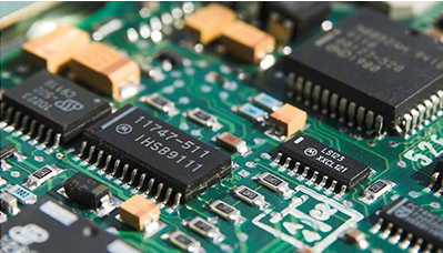
2. Procurement and inspection of components
The procurement of components requires strict control of channels, and must be picked up from large traders and original factories, and 100% avoid second-hand materials and fake materials. In addition, a special inspection post for incoming materials is set up, and the following items are strictly inspected to ensure that the components are free of faults.
PCB: Reflow soldering furnace temperature test, no flying leads, whether the vias are blocked or leaking ink, whether the board surface is bent, etc.
IC: Check whether the silk screen is completely consistent with the BOM, and keep it at constant temperature and humidity
Other common materials: check silk screen, appearance, power-on measurement, etc. The inspection items are carried out according to the sampling method, and the ratio is generally 1-3%
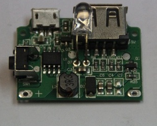
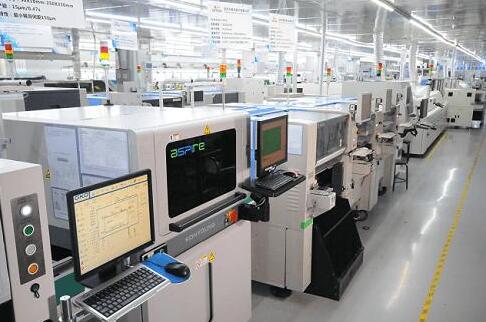
3. SMT Assembly processing
Solder paste printing and reflow oven temperature control are key points, and it is very important to use laser stencils of good quality and meeting process requirements. According to the requirements of PCB, some steel mesh holes need to be enlarged or reduced, or U-shaped holes are used to make steel mesh according to process requirements. The furnace temperature and speed control of the reflow soldering is very critical to the solder paste infiltration and soldering reliability. It can be controlled in accordance with the normal SOP operation guidelines. In addition, AOI testing needs to be strictly implemented to minimize the defects caused by human factors.
4. Plug-in processing
In the plug-in process, the mold design for wave soldering is a key point. How to use molds to maximize the probability of good products after the furnace is a process that PE engineers must continue to practice and summarize experience.
5. Program firing
In the previous DFM report, customers can be suggested to set up some test points (Test Points) on the PCB, the purpose is to test the PCB and PCBA circuit continuity after soldering all components. If you have conditions, you can ask the customer to provide a program, and burn the program into the main control IC through a burner (such as ST-LINK, J-LINK, etc.), and you can more intuitively test the effects of various touch actions. Functional changes to verify the functional integrity of the entire PCBA.