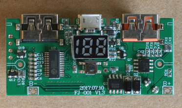
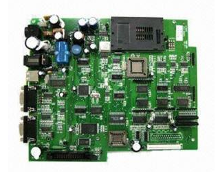
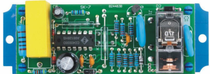
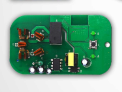
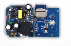
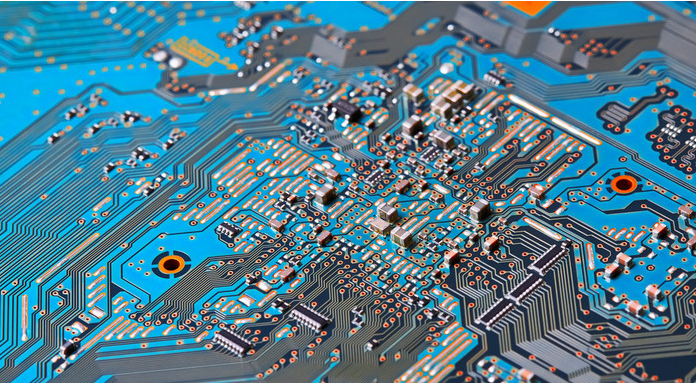
SMT: Abbreviation of English Surface Mount Technology, Chinese means surface mount welding (mounting) technology, the technology of soldering electronic parts to the surface of the circuit board. As a new generation of electronic assembly technology, SMT products have the advantages of compact structure, small size, vibration resistance, and high production efficiency. SMT has occupied a leading position in the circuit board assembly process. The main equipment of the SMT assembly line: printing Machine, placement machine, reflow soldering, etc.
Why is smt patch processing technology so popular? Advantages of SMT chip processing:
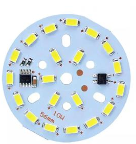
1. Electronic products are small in size and high in assembly density
The volume of SMT chip components is only about 10% of traditional package components, and the weight is only 10% of traditional plug-in components.
2. High reliability and strong anti-vibration ability
SMT chip processing uses chip components, which have high reliability, small size, light weight, strong anti-vibration ability, automatic production, high installation reliability, and low solder joint defect rate.

3. Good high frequency characteristics and reliable performance
Because the chip components are firmly mounted, the devices are usually leadless or short leads, which reduces the influence of parasitic inductance and parasitic capacitance, improves the high-frequency characteristics of the circuit, and reduces electromagnetic and radio frequency interference.
4. Improve productivity and realize automated production
The automatic placement machine (Yamaha automatic placement machine ysm-10/ysm-20) uses a vacuum nozzle to suck and release the components. The vacuum nozzle is smaller than the shape of the component, which improves the installation density.
5. Reduce costs and reduce expenses
SMT patch processing technology can save materials, energy, equipment, manpower, time, etc., and the cost can be reduced by up to 30% and 50%! !
It is precisely because of the complexity of the process flow of SMT chip processing that there are many SMT chip processing factories that specialize in SMT chip processing.
Professional soldering method of SMT chip
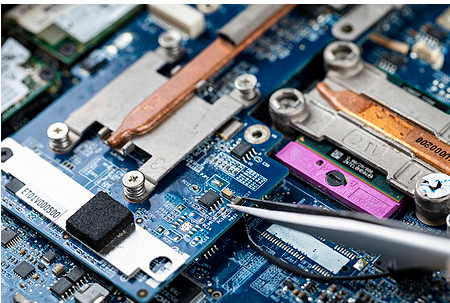
1. First, clamp the chip with tweezers and align the pads:
For the needs of electronic enthusiasts, the Chuangfu platform provides a free e-learning platform, mainly to allow more electronic enthusiasts to get started quickly. Our platform has many years of senior engineers, R&D RD, FAE failure analysis engineers, powerRD, HardwareRD, SoftwareRD, senior automation RD, technical director, etc., in order to integrate the development of social positions and factories
2. Then press the chip with your thumb:
Before proceeding to the next step, be sure to confirm that the chip has been aligned to the pad, otherwise it will be more troublesome to find that the chip is not aligned after the next step. Then use tweezers to take a small piece of rosin and place it next to the pins of the D12 chip. Note that rosin is used here, not the thick flux (this flux can't hold the chip):
4. The next step is to melt the rosin with a soldering iron. Rosin has two functions here: one is to fix the chip on the PCB, and the other is to help solder, haha. When melting the rosin, it is necessary to dissolve the rosin as much as possible and distribute it evenly on a row of pads.
5. Then use rosin to fix the pins on the other side of D12. After this step, D12 will be firmly fixed on the PCB, so before you check whether the chip is accurately aligned with the pads, or wait for the rosin on both sides to be applied. It's not very easy to take after it's done.
6. If you accidentally put too much at once, it is not without a solution. If it is just a little more, you can drag left and right as shown in the video tutorial to make the excess tin evenly distributed to each pad to solve the problem; if A lot more, you need to use other methods, it is recommended to use a suction tape to get the excess solder out
7. Use a soldering iron to melt the solder, and then drag the soldering iron to the right along the contact point of the pin and the pad until it reaches the rightmost pin:
For example, the pins on one side of D12 are all soldered, and the other side can be soldered with the same method. At the same time, you can also refer to the following video for practice.