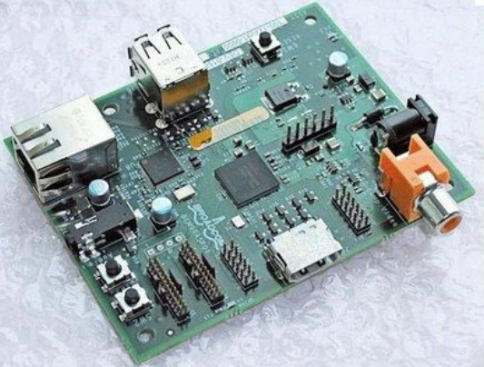
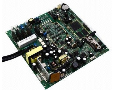
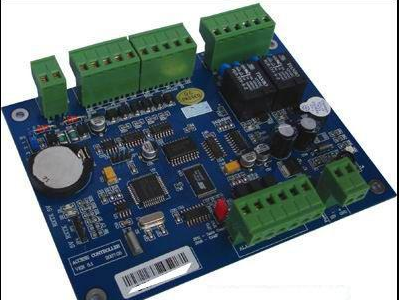
Manual maintenance skills in the maintenance of smt patch processing plants
Although the smt patch processing is now automated, it does not mean that no manual work is required. In fact, manual operation is inevitable in the process of smt patch processing and maintenance. Therefore, as an operator, you must master manual maintenance skills. So, what are the manual repair skills in smt patch processing and repair? Let me talk about it in detail below.
1. Tools and materials
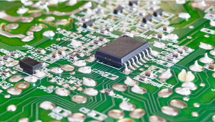
In general, there are two common manual repair methods, one is contact welding repair, the other is heating gas welding repair. The contact welding repair method is to directly touch the solder joints on the heated soldering iron tip or soldering iron ring. Soldering iron rings are more suitable for removing glue-bonded components. They are effective for rectangular or cylindrical components and integrated circuits, but have little effect on four-sided plastic-encapsulated components.
In the manual soldering repair process, flux and solder paste are needed, the purpose of which is to prevent the solder, component pins, pads, etc. from being rapidly oxidized. At the same time, the solder on the pad is used for soldering to fix the components and reduce the occurrence of false soldering and continuous soldering failures.

In addition to the main tools and materials, manual maintenance also requires some auxiliary tools and materials, such as tweezers, vacuum suction pens, suction tape for cleaning pads, and magnifying glasses for quality inspection.
Two, smt patch processing and maintenance methods
Type 1: Under the premise of not having a hot air gun, choose a pincer-shaped soldering iron, and clamp the component with a pincer-shaped soldering iron on the IC side to prevent it from shifting. The heat of the soldering iron tip will be transferred to each pin after it has melted. Therefore, it must be noted that the PLCC components removed by this method cannot be reused, and the high temperature that melts in a large area can easily cause damage to the circuit board. In addition, the low cost of the pincer-shaped soldering iron is relatively high, and the weak smt chip processing manufacturers generally do not have it.
The second type: Blow welding with a hot air gun. After all the lead solders have melted, remove the IC, and then clean it up with a soldering tape.
In smt patch processing and maintenance, manual operation is much easier than machine disassembly, and this method can also ensure that the loss of components is lower. Not only that, because it is manual maintenance, so based on experience and professional knowledge, we can better judge the maintenance situation, make appropriate responses according to the specific situation, remedy, and reduce losses.
It is worth noting that the circuit boards of the game industry are coated with protective glue for the purpose of waterproof and shockproof. In the manual repair process, after the solder has melted, the protective glue must be removed with the tool in the hand before removing the components. In addition, in the next operation, pay attention to the glue, otherwise the components will not be firmly fixed.
Warm reminder: The smt patch processing and maintenance are performed manually, and you must have enough patience and operating skills. Beginners only need to be proficient to operate. Therefore, when choosing an smt patch processing and repair factory, you must choose a professional, regular, and powerful manufacturer, so as to ensure the repair effect and ensure the quality of future products.
"Questioning" Answers to PCB Proofing Questions
PCB is the abbreviation of printed circuit board, and PCB proofing is to produce small quantities of samples for testing before mass production. This also answers the market's questions about what PCB proofing is. Many electronic manufacturing companies will find some professional PCB proofing manufacturers to cooperate, so what are the problems that need to be paid attention to in the PCB proofing process?
1. Pay attention to the number of samples
Before large-scale mass production, companies often need to make a batch of PCB prototypes for testing, and this part actually occupies a certain cost of the company, especially when the company is large and produces many types of PCBs, then PCB proofing and testing The cost is also extremely considerable. From this point of view, companies should pay attention to the number of samples in the PCB proofing process.
Second, confirm the device package
Soldering a chip with a specific function on the circuit board and encapsulating it with a shielding cover is a process in the manufacturing process of the circuit board. In the process of PCB proofing, the client should pay great attention to whether the internal chips and electronic components are incorrectly soldered during packaging, so as to ensure the quality of PCB proofing, and then be able to verify the function and follow-up further large-scale production.
Third, do a comprehensive electrical inspection
After the PCB proofing, the company should conduct a comprehensive electrical inspection to ensure that every function and every detail of the PCB board is checked. This is the significance of the PCB proofing, and it is also whether the subsequent PCB board can be put into mass production on a large scale and ensure extremely low defects Where the rate is guaranteed. To do a comprehensive electrical inspection, it is recommended that the client and the proofing party cooperate to carry out the investigation is a more rigorous testing method.
Of course, there are some signal integrity layouts that need to be paid attention to and resolved by both parties, but in general, the issues that need to be paid attention to in PCB proofing are roughly the above-mentioned items. Although there are many doubts in the market about what PCB proofing means, as an industry insider, thorough investigation and testing of the above-mentioned problems is the basis for ensuring the quality of PCB samples and converting them into subsequent mass production. For PCB Proofing must be taken fully and seriously.