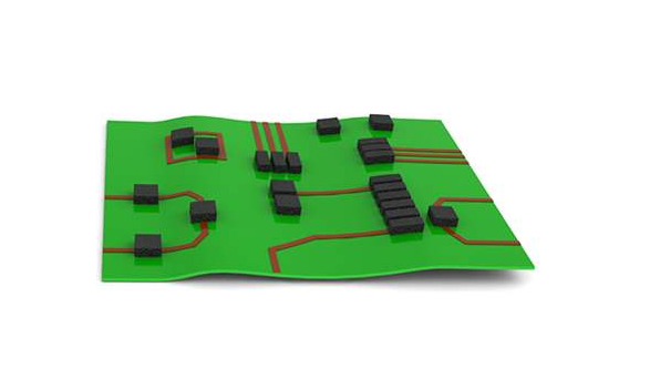
For this BGA problem, the root cause is insufficient solder paste. Another common cause of imperfect solder joints in PCBA BGA rework is the capillary phenomenon of the solder. BGA solder flows into the through hole due to the capillary effect to form information. Chip offset or printed tin offset, BGA pads and defective vias without solder mask isolation may cause capillary phenomena, resulting in incomplete BGA solder joints. Especially in the repair process of BGA devices, if the solder mask is damaged, the capillary phenomenon will be aggravated, leading to the formation of imperfect solder joints.
Incorrect PCB design can also lead to incomplete solder joints. If there is a hole in the BGA pad, most of the solder will flow into the hole. If the amount of solder paste provided is insufficient, a low-support solder joint will be formed. The remedy is to increase the amount of solder paste printed. When designing the stencil, the amunt of solder paste absorbed by the holes on the disc should be considered. By increasing the thickness of the stencil or increasing the size of the opening of the stencil, a sufficient amount of solder paste can be ensured. Another solution is to use micro-hole technology to replace the hole design in the disk to reduce the loss of solder.

Another factor leading to incomplete solder joints is the poor coplanarity between the device and the printed circuit board. If the printing volume of solder paste is sufficient. But the gap between BGA and PCB is inconsistent, that is, poor coplanarity will lead to imperfect solder joints. This situation is especially common in CBGA.
PCBA patch processing BGA solder joint incomplete solution
1. Print enough solder paste;
2. Cover the through holes with solder resist to avoid solder loss;
3. Avoid damaging the solder mask during the BGA repair stage of PCBA processing;
4. Accurate alignment of the color tone when printing solder paste;
5. The accuracy of BGA placement;
6. Correct operation of BGA components in the repair phase;
7. Meet the coplanarity requirements of PCB and BGA and avoid warpage. For example, proper preheating can be adopted in the repair stage;
8. Micro-hole technology is used to replace the hole design on the disc to reduce the loss of solder.
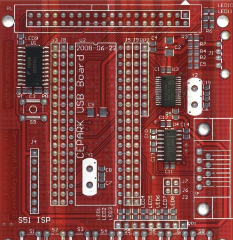
SMT chip processing solder joint quality
1. Judgment of Welding
1. Use online tester professional equipment for testing.
2. Visual inspection or AOI inspection. When you find that the solder joints have too little solder material, the solder penetration is poor, or there are cracks in the middle of the solder joints, or the surface of the solder is convex spherical, or the solder does not melt with the SMD, etc., you need to pay attention to it, even if it is a slight condition Causes hidden dangers, it should be immediately judged whether there is a lot of false welding problem. The method of judgment is: to see if there are many solder joints at the same position on the PCB, such as the problem on some PCBs, it may be due to scratching of the solder paste, pin deformation, etc., such as on many PCBs. There is a problem with the same position. At this time, it is likely to be caused by a bad component or a problem with the pad.
Second, the cause of the virtual welding and its solution
1. The pad design is defective. The existence of through-holes in the pads is a major disadvantage of PCB design. If it is not necessary, it is not necessary to use them. The through-holes will cause the loss of solder and lead to insufficient soldering materials. The spacing and area of the pads also need to be standardized, otherwise the design should be corrected as soon as possible.
2. The PCB board is oxidized, that is, the pad is black and does not shine. If there is oxidation, you can use an eraser to remove the oxide layer to make it bright again. If the PCB board is damp, it can be dried in a drying box if suspected. The PCB board has oil stains, sweat stains and other pollution, so use absolute ethanol to clean it up.
3. For PCBs that have been printed with solder paste, the solder paste is scraped and rubbed, which reduces the amount of solder paste on the relevant pads and makes the soldering material insufficient. Should be added immediately. You can use a dispenser or use a bamboo stick to pick a little supplement.