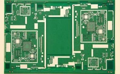
The production of stencil is very important to the SMT chip processing technology. It will directly determine whether the tin on each pad is uniform and full, which will affect the soldering reliability of SMT components after reflow soldering after mounting. Generally speaking, it is necessary to carefully analyze the characteristics of each PCB to develop steel mesh. For some high-precision and quality-required circuit boards, laser steel mesh must be used, and SMT engineers are required to discuss and confirm the process after meeting to adjust the opening appropriately. The hole diameter ensures the tinning effect.
When making SMT steel mesh, generally pay attention to:
1.ME requires the supplier to make steel mesh according to the relevant documents and information provided by the engineering department.
2. The frame size requirements of the steel mesh (550MM*650MM 370MM*470MM, etc., mainly based on the structure of the printing press and product specifications)
3. The markings on the steel mesh (product model, thickness, production date, etc.)

4. The thickness of the steel mesh (usually 0.18MM-0.2MMM for squeegee, 0.1MM-0.15MM for tinning)
5. The opening method and size of the steel mesh (the anti-tin ball is generally V-shaped, U-shaped, concave, etc., depending on the type of each component.)
6. The direction of the board and the placement machine should be unified
SMT steel mesh acceptance notes:
1. Check whether the method and size of the steel mesh opening meet the requirements
2. Check whether the thickness of the steel mesh meets the product requirements
3. Check whether the frame size of the steel mesh is correct
4. Check whether the marking of the steel mesh is complete
5. Check whether the flatness of the steel mesh is level
6. Check whether the tension of the steel mesh is OK
7. Check whether the position and number of openings in the steel mesh are consistent with the GERBER file
Steel mesh production is an important part of the quality control of the entire SMT patch processing process. Engineers must pay full attention to it. Customers should not deliberately reduce costs, resulting in poor tin application after using the steel mesh, which affects the entire production schedule.
SMT chip processing solder joint quality
1. Judgment of Welding
1. Use online tester professional equipment for testing.
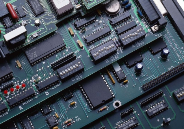
2. Visual inspection or AOI inspection. When you find that the solder joints have too little solder material, the solder penetration is poor, or there are cracks in the middle of the solder joints, or the surface of the solder is convex spherical, or the solder does not melt with the SMD, etc., you need to pay attention to it, even if it is a slight condition Causes hidden dangers, it should be immediately judged whether there is a lot of false welding problem. The method of judgment is: to see if there are many solder joints at the same position on the PCB, such as the problem on some PCBs, it may be due to scratching of the solder paste, pin deformation, etc., such as on many PCBs. There is a problem with the same position. At this time, it is likely to be caused by a bad component or a problem with the pad.
Second, the cause of the virtual welding and its solution
1. The pad design is defective. The existence of through-holes in the pads is a major disadvantage of PCB design. If it is not necessary, it is not necessary to use them. The through-holes will cause the loss of solder and lead to insufficient soldering materials. The spacing and area of the pads also need to be standardized, otherwise the design should be corrected as soon as possible.
2. The PCB board is oxidized, that is, the pad is black and does not shine. If there is oxidation, you can use an eraser to remove the oxide layer to make it bright again. If the PCB board is damp, it can be dried in a drying box if suspected. The PCB board has oil stains, sweat stains and other pollution, so use absolute ethanol to clean it up.
3. For PCBs that have been printed with solder paste, the solder paste is scraped and rubbed, which reduces the amount of solder paste on the relevant pads and makes the soldering material insufficient. Should be added immediately. You can use a dispenser or use a bamboo stick to pick a little supplement.