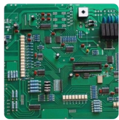
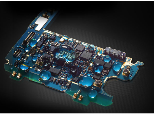
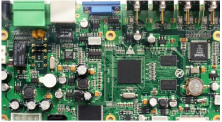
In production, if there is a lot of solder after encountering, then you need to choose wave soldering for processing. When operating wave soldering, you need to pay attention to:
The wave crest surface is covered by a layer of oxide scale, which is almost static along the entire length of the solder wave. During the wave soldering process, the PCB touches the front surface of the tin wave, the oxide scale is broken, and the tin wave in front of the PCB is not The folds are pushed forward, which shows that the entire oxide skin moves at the same speed as the PCB.
Generally, in order to avoid poor wave soldering, the following methods can be used to avoid: Use components/PCBs with good solderability, increase the activity of soldering, increase the preheating temperature of the PCBA, increase the wettability of the pad, and increase the temperature of the solder, Remove harmful impurities, reduce the cohesion of the solder, in order to facilitate the separation of the solder between the two solder joints.

Common preheating methods in wave soldering machines: air convection heating, infrared heater heating, heating by a combination of hot air and radiation; wave soldering process curve analysis: wetting time refers to the start of wetting after the solder joints contact the solder Time and residence time refer to the time from contacting the crest surface to leaving the crest surface of a solder joint on the PCB. The preheating temperature refers to the temperature reached before the PCB and the crest surface contact, and the soldering temperature refers to the very high soldering temperature. Important welding parameters. Usually 50°C ~ 60°C higher than the melting point of the solder (183°C). Most cases mean that the temperature of the soldering furnace is lower than the temperature of the soldering point of the PCB during actual operation. This is due to the heat absorption of the PCB. .
How to calculate the cost of PCBA patch processing factory?
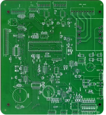
1. PCB board fee
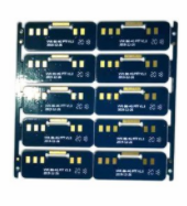
If you want to find a PCBA processor to help you process, then you have to provide the PCB file and BOM list, and the PCBA processor will help you make the bare PCB board according to your PCB file. At this time, the first part of the cost will be incurred, the PCB board. fee. The cost of the PCB board is determined by the difficulty of the board. For example, 4-layer board, 8-layer board, aluminum substrate, carbon ink board, the prices of these boards are different. Of course, you can also find a PCBA board factory for processing. The price is definitely not that cheap. After all, someone else has a long-term cooperation. There must be a discount. The local tyrants please feel free.
2. Component purchase fee
The second part of the cost of PCBA patch processing, the purchase of components. The processing manufacturer purchases the components you need according to the BOM. When the components are purchased, due to the loading of the disk such as resistors and capacitors and the loss of the SMT patch (such as the wrong board, the tape is not cleared in time, etc.), it needs to be covered About 5% of material loss rises; processing manufacturers have long-term cooperation with component manufacturers, so the price will be lower.
3. SMT processing fee (SMD patch + DIP post welding)
When calculating the SMT processing fee, you must first see how large your processing batch is. If it is greater than 2000pic, there is no need to charge engineering fees, otherwise engineering fees will be charged. Next, calculate the number of points and multiply the unit price of the points. The unit price of the patch points is between 0.01-0.015 yuan. The calculation of the points is calculated according to the SMT patch material 2 feet and 1 point, and the DIP plug-in 1 foot and 1 point. Multiply the two together. Refinement can be divided:
1.0402 components are calculated at RMB 0.015 per point. 0603-1206 components are calculated at RMB 0.015 per point
2. One foot of the plug-in material is one point; it is calculated at RMB 0.015 per point.
3. The slot type has 4 pins as 1 point; it is calculated at RMB 0.015 per point.
4. Ordinary IC, 4 pins are 1 point; it is calculated at RMB 0.015 per point.
5. Close-pin IC, 2 pins are 1 point; it is calculated at RMB 0.015 per point.
6. 2 feet of BGA is 1 point; it is calculated at RMB 0.015 per point.
7. Machine-mounted large materials are calculated according to the volume of the components doubled.
8. The additional fee is calculated at RMB 20 per hour
9. This quotation does not include testing fees, transportation fees, taxes, etc.
Four, PCBA test fee and assembly fee
The PCBA test fee is generally calculated at 2 yuan per board, plus PCBA assembly and packaging costs, generally 0.8 yuan/piece, this is the fourth part of the cost.
Now, add up the cost of the above four parts, it is the PCBA patch processing cost!