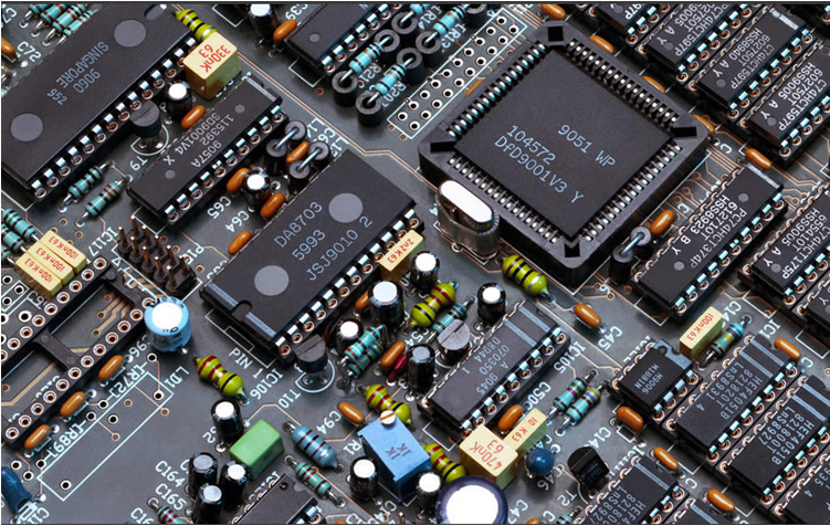
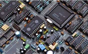
The SMT assembly process is closely related to each process step before soldering, including capital investment, PCB design, component solderability, assembly operations, flux selection, temperature/time control, solder and crystal structure, etc.
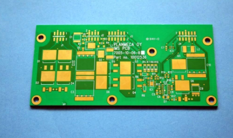
1. PCB solder
At present, the most commonly used solder for wave soldering is eutectic tin-lead alloy: tin 63%; lead 37%. The temperature of the solder in the soldering pot should be kept at all times, and the temperature should be higher than the alloy liquid temperature of 183 degree Celsius, and the temperature should be uniform. In the past, the solder pot temperature of 250°C was regarded as the "standard".
With the innovation of flux technology, the uniformity of the solder temperature in the entire solder pot has been controlled, and a preheater has been added. The development trend is to use temperature

A solder pot with a lower temperature. It is very common to set the solder pot temperature in the range of 230-240 degree Celsius. Generally, components do not have uniform thermal quality, and it is necessary to ensure that all solder joints reach a sufficient temperature in order to form qualified solder joints. The important issue is to provide enough heat to increase the temperature of all leads and pads, thereby ensuring the fluidity of the solder and wetting both sides of the solder joint. The lower temperature of the solder will reduce the thermal shock to the components and the substrate, which will help reduce the formation of scum. Under the lower strength, the joint action of the flux coating operation and the flux compound can make the wave outlet have Enough flux, so that burrs and solder balls can be reduced.
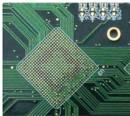
The solder composition in the solder pot is closely related to time, that is, changes with time, which leads to the formation of scum. This is the reason for removing residues and other metal impurities from the soldered components and in the soldering process. Causes of tin loss. These factors can reduce the fluidity of the solder. In procurement, the maximum limit of tin content in metal trace dross and solder must be specified in various standards (for example, IPC/J-STD-006 has clear regulations). During the soldering process, the requirements for solder purity are also specified in the ANSI/J-STD-001B standard. In addition to the restriction on dross, 63% tin; 37% lead alloy stipulates that the tin content shall not be less than 61.5%. The concentration of gold and copper in the organic bathing layer on the wave soldering components accumulate faster than in the past. This accumulation, coupled with significant tin loss, can cause the solder to lose fluidity and cause soldering problems. Rough, granular solder joints are often caused by scum in the solder. Dim and rough granular solder joints due to the accumulated scum in the solder pot or the inherent residue of the component itself may also be a sign of low tin content. It is not a local special solder joint or the result of tin loss in the tin pot. This appearance may also be caused by vibration or shock during the solidification process.
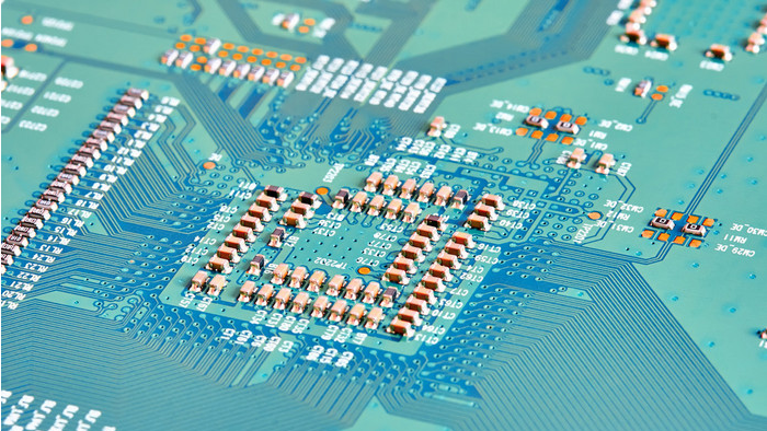
The appearance of the solder joints can directly reflect process or material problems. In order to maintain the solder "full pot" state and check the solder according to the process control plan
Pot analysis is very important. Because there is scum in the solder pot, it is usually unnecessary to "pour out" the flux in the solder pot. In conventional applications, it is required to add solder to the solder pot, so that the solder in the pot is always full. . In the case of loss of tin, the addition of pure tin helps to maintain the desired concentration. In order to monitor the compounds in the tin pot, routine analysis should be performed. If tin is added, samples should be sampled and analyzed to ensure that the solder composition ratio is correct. Excessive scum is another thorny problem. There is no doubt that scum is always present in the solder pot, especially when soldering in the atmosphere. Using "chip crests" is very helpful for soldering high-density components, because the solder surface exposed to the atmosphere is too large, and the solder oxidizes, so more scum will be generated. The surface of the solder in the solder pot is covered by a scum layer, and the oxidation rate slows down.
During soldering, more scum is generated due to the turbulence and flow of wave crests in the tin pot. The recommended conventional method is to skim the scum. If skimming is done frequently, more scum will be produced and more solder will be consumed. The scum may also be mixed in the wave crests, causing instability or turbulence in the wave crests. Therefore, more maintenance is required for the liquid components in the solder pot. If it is allowed to reduce the amount of solder in the tin pot, scum on the surface of the solder will enter the pump, and this phenomenon is likely to occur. Sometimes, granular solder joints will be mixed with dross. The initial scum found may be caused by rough wave crests and may clog the pump. The tin pot should be equipped with an adjustable low-volume solder sensor and alarm device.
2 crest
In the wave soldering process, the wave crest is the core. The preheated, flux-coated, and non-contaminated metal can be sent to the welding station through the conveyor belt to contact
The solder with a certain temperature is then heated, so that the solder will have a chemical reaction, and the solder alloy will form interconnections through wave power. This is the most critical step. At present, the commonly used symmetrical wave crest is called the main wave crest. The pump speed, wave crest height, infiltration depth, transmission angle and transmission speed are set to provide a full range of conditions for achieving good soldering characteristics. The PCB data should be adjusted appropriately, and the solder should be slowed down after leaving the crest (outlet end), and the operation should be stopped slowly. The PCB will eventually push the solder to the outlet as the wave runs. In the most hanging condition, the surface tension of the solder and the optimized board peak operation can achieve zero relative motion between the component and the wave peak at the exit end. This shelling area is to achieve the removal of solder on the board. Sufficient inclination angle should be provided, and no defects such as bridging, burrs, wire drawing and solder balls should be produced. Sometimes, the exit of the wave crest needs to have hot air flow to ensure that possible bridges are eliminated. After mounting surface mount components on the bottom of the board, sometimes to compensate for the flux or bubbles in the "harsh wave crest" area formed later, and before the wave crest is leveled, the turbulent chip crest is used. The high vertical velocity of the turbulent wave crest helps to ensure the contact of the solder with the lead or pad. The vibrating part behind the flattened laminar wave peak can also be used to eliminate air bubbles and ensure that the solder achieves satisfactory contact with the component. The soldering station should basically: high-purity solder (according to the standard), peak temperature (230~250 degree Celsius), total contact time (3~5 seconds), the depth of the printed board immersed in the wave peak (50~80 %), to realize the parallel transmission track and the flux content in the tin pot when the wave crest is parallel to the track.
3 Cooling after wave soldering
A cooling station is usually added to the tail of the wave soldering machine. In order to limit the tendency of copper-tin intermetallic compounds to form solder joints, another reason is to accelerate
The cooling of the components prevents the board from shifting when the solder is not completely solidified. Quickly cool components to limit exposure of sensitive components to high temperatures. However, consideration should be given to the hazards of the thermal shock of the aggressive cooling system to the components and solder joints. A well-controlled "soft and stable", forced air cooling system should not damage most PCB components. There are two reasons for using this system: the board can be processed quickly without holding it by hand, and it can ensure that the temperature of the components is lower than the temperature of the cleaning solution. People are concerned about the latter reason, which may be the cause of foaming of some flux residues. Another phenomenon is that it sometimes reacts with certain flux scum, so that the residue is "unwashable". In terms of ensuring that the data set by the welding workstation meets all the machines, all the PCB designs, all the materials used, and the material conditions and requirements of the PCB process, no formula can meet these requirements. Must understand every step of the operation in the entire PCB process.