The surface adhesion assembly process of SMT chip processing, especially for small pitch components, requires continuous monitoring of the process and systematic inspection. For example, currently in the United States, the quality standard for solder joints is based on IPC-A-620 and the national solder standard ANSI/J-STD-001. Knowing these guidelines and specifications, designers can develop products that meet the requirements of industry standards.
The surface adhesion assembly process of smt chip processing, especially for small pitch components, requires continuous monitoring of the process and systematic inspection. For example, currently in the United States, the quality standard for solder joints is based on IPC-A-620 and the national solder standard ANSI/J-STD-001. Knowing these guidelines and specifications, designers can develop products that meet the requirements of industry standards.
Mass production design
The mass production design includes all the mass production process, assembly, testability and reliability, and is based on the written document requirements as the starting point.
A complete and clear assembly document is absolutely necessary and a guarantee of success for a series of conversions from design to manufacturing. The list of related documents and CAD data includes a bill of materials (BOM), a list of qualified manufacturers, assembly details, special assembly guidelines, PC board manufacturing details, and the disk containing Gerber data or IPC-D-350 program.

The CAD data on the disk is of great help to the development of testing and manufacturing process tools, and the preparation of automated assembly equipment programs. It includes the X-Y axis coordinate position, test requirements, summary graphics, circuit diagram and X-Y coordinates of the test point.
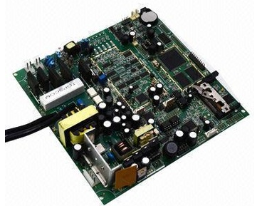
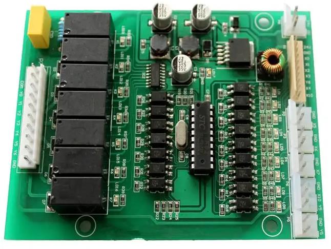
PCB board quality
From each batch or a specific batch number, take a sample to test its solderability. This PC board will first be compared with the product information provided by the manufacturer and the quality specifications calibrated on the IPC. The next step is to print the solder paste on the solder pad and reflow. If an organic flux is used, it needs to be cleaned to remove the residue. While evaluating the quality of solder joints, the appearance and size of the PC board should also be evaluated together after reflow. The same inspection method can also be applied to the wave soldering process.
Assembly process development
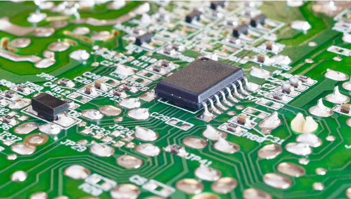
This step involves uninterrupted monitoring of every mechanical action with the naked eye and automated visual devices. For example, it is recommended to use a laser to scan the volume of solder paste printed on each PC board.
After placing the sample on the surface mount component (SMD) and reflowing, the quality control and engineering personnel need to check the tin consumption on the pins of each component one by one, and each member needs to record the passive components and the multi-pin components in detail. The counterpoint situation. After the wave soldering process, it is also necessary to carefully inspect the uniformity of the soldering and determine the potential locations of solder joints that may cause defects due to the pitch or component distance too close.
Fine pitch technology
Fine pitch assembly is an advanced construction and manufacturing concept. The component density and complexity are far greater than those of mainstream products in the current market. If it is to enter the mass production stage, some parameters must be revised before it can be put into the production line.
The dimensions and spacing of the solder pads generally follow the IPC-SM-782A specifications. However, in order to meet the requirements of the manufacturing process, the shape and size of some pads will be slightly different from this specification. For wave soldering, the pad size is usually slightly larger in order to have more flux and solder. For some components that are usually kept near the upper and lower limits of the process tolerance, it is necessary to adjust the size of the solder pads appropriately.
Consistency of placement of surface mount components
Although it is not entirely necessary to design all the components in the same position, for the same type of components, the consistency will help improve the efficiency of assembly and inspection. For a complex board, components with pins usually have the same placement to save time. The reason is that the grab heads for placing components are usually fixed in one direction, and the board must be rotated to change the placement direction. As for general surface adhesive components, because the grab head of the placement machine can rotate freely, there is no problem in this respect. But if you want to go through the wave soldering furnace, the components must be aligned to reduce the time they are exposed to the tin flow.
The polarity of some polarized components is determined as early as the entire circuit design. After the process engineer understands the circuit function, deciding the order of placing the components can improve the assembly efficiency, but there is a consistent directionality. Or similar components can improve its efficiency. If the placement position can be unified, not only the speed of writing and placing component programs can be shortened, but also the occurrence of errors can be reduced at the same time.
Consistent (and sufficient) component distance
Fully automatic surface mount component placement machines are generally quite accurate, but designers tend to ignore the complexity of mass production while trying to increase component density. For example, when a tall component is too close to a component with a fine pitch, it will not only block the line of sight to inspect the solder joints of the pins, but also hinder the heavy work or tools used during heavy work.
Wave solder is generally used in relatively low and short components such as diodes and transistors. Small components such as SOIC can also be used in wave soldering, but it should be noted that some components cannot withstand direct exposure to the high heat of the tin furnace.
In order to ensure the consistency of the assembly quality, the distance between the components must be large enough and evenly exposed to the tin furnace. In order to ensure that the solder can touch each contact, a certain distance should be kept between tall components and low and low components to avoid the shadowing effect. If the distance is insufficient, it will also hinder the inspection of components and heavy work.
The industry has developed a set of standard applications for surface mount components. If possible, use standard-compliant components as much as possible, so that designers can build a database of standard solder pad sizes, so that engineers can better understand process problems. Designers can find that some countries have established similar standards, and the appearance of the components may be similar, but the lead angles of the components are different depending on the country of manufacture. For example, SOIC component suppliers from North America and Europe can meet the EIZ standard, while Japanese products are based on EIAJ as its design criteria. It should be noted that even if it conforms to the EIAJ standard, the appearance of components produced by different companies is not exactly the same.
Designed to improve production efficiency
Assembling the board can be quite simple or very complex, depending on the shape and density of the components. A complex design can be made into efficient production and reduce the difficulty, but if the designer does not pay attention to the details of the process, it will become very difficult. The assembly plan must be considered at the beginning of the design. Generally, as long as the position and placement of the components are adjusted, the mass productivity can be increased. If a PCB board is small in size, has an irregular shape or has components very close to the edge of the board, consider mass production in the form of connected boards.