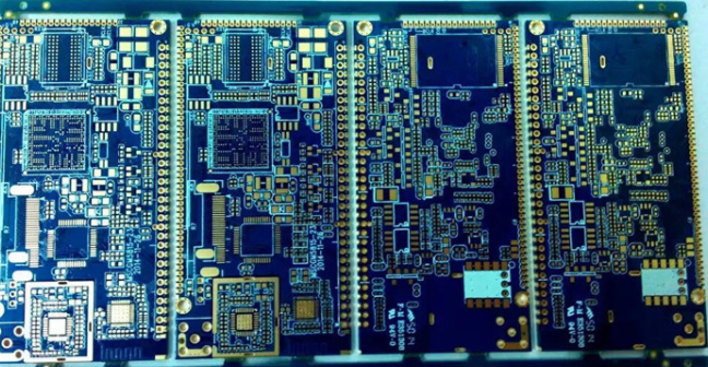
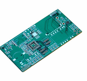
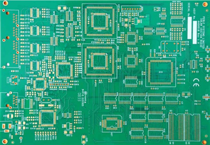
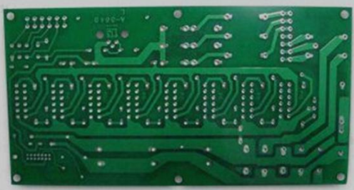
In the PCBA processingprocess, the most commonly used mounting technology is SMT chip processing technology. SMT chip processing is a circuit assembly technology that attaches and solders surface mount components to a specified position on the surface of a printed circuit board. It is widely used in large circuit board manufacturers and is currently the most popular technology and process.
1. Reasons for using PCBA to process surface mount technology (SMT):
1. Electronic products are pursuing miniaturization, and the previously used perforated plug-in components can no longer be reduced;
2. Electronic products have more complete functions. The integrated circuits (ICs) used have no perforated components, especially large-scale and highly integrated ICs, so surface mount components have to be used;
3. Mass production of products and automation of production. The factory must produce high-quality products with low cost and high output to meet customer needs and strengthen market competitiveness;

4. The development of electronic components, the development of integrated circuits (IC), the diversified application of semiconductor materials, and the electronic technology revolution is imperative to pursue the international trend.
2. Advantages of SMT chip processing:
1. High reliability, strong anti-vibration ability, and low solder joint defect rate;
2. Good high frequency characteristics, reducing electromagnetic and radio frequency interference;
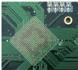
3. High assembly density, small size and light weight of electronic products. The volume and weight of SMT components are only about 1/10 of traditional plug-in components. Generally, after SMT is adopted, the volume of electronic products is reduced by 40% to 60%, and the weight is reduced by 60%. %~80%;
4. It is easy to realize automation, improve production efficiency, reduce costs by 30%~50%, and save materials, energy, equipment, manpower, time, etc.
3. Technical composition related to SMT patch processing:
1. Design and manufacturing technology of electronic components and integrated circuits;
2. Circuit design technology of electronic products;
3. The manufacturing technology of the circuit board;
4. Design and manufacturing technology of automatic placement equipment;
5. Circuit assembly manufacturing process technology;
6. Development and production technology of auxiliary materials used in assembly manufacturing.
SMT chip processing device cracking solution
Reasons for cracking of SMT chip processing devices
1. For MLCC capacitors, their structure is made up of multilayer ceramic capacitors, so their structure is weak, low strength, strong heat resistance and mechanical impact, which is especially obvious in wave soldering.
2. During the SMT placement process, the suction and release height of the Z-axis of the placement machine, especially some placement machines that do not have the Z-axis soft landing function, the absorption height depends on the thickness of the chip component, not through the pressure sensor, so Tolerances in component thickness can cause cracks.
3. After soldering, if there is warping stress on the PCB, it is easy to cause the components to crack.
4. PCB stress during splicing can also damage components.
5. The mechanical stress during the ICT test caused the device to rupture.
6. The stress during assembly can cause damage to the MLCC around the fastening screw.
SMT chip processing device cracking scheme
1. Carefully adjust the welding process curve, especially the heating speed should not be too fast.
2. During the placement, please ensure proper placement of the machine pressure, especially for thick plates and metal substrates, as well as ceramic substrates to install MLCC and other brittle devices, pay special attention.
3. Pay attention to the placement method and shape of the cutter.
4. The warpage of the PCB, especially the warpage after soldering, should be specially corrected to prevent the stress caused by the large deformation from affecting the device.
5. During PCB design, avoid high stress areas of MLCC and other devices.