In smt patch processing, it is not only the placement of components on the designated PCB pads. If you want to get good quality and customer reputation, obviously this is not enough. We must obtain enough data through various testing methods to obtain specific testing data and records to support our quality requirements. At this time, various detection techniques and methods become very important.
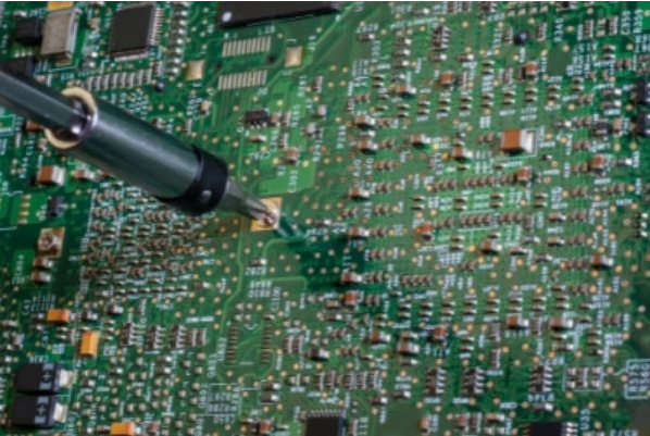
From the perspective of the smt processing plant, talk about the related issues of online testing (ICT). In-circuit test (ICT) is usually used to detect the direction of the circuit board, such as open circuit, resistance, capacitance and components, but it is also a relatively seldom used device. What are the specific advantages and disadvantages?
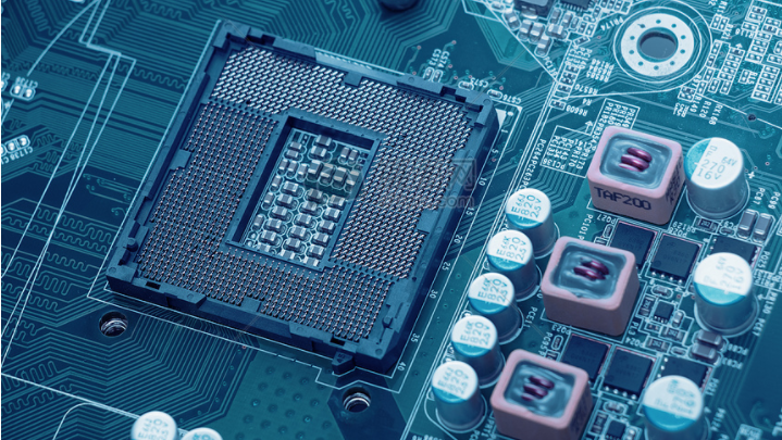
ICT test
As we all know, online testing or ICT works by using a bunch of probes to access circuit nodes, and then check the performance of each component. It can also test the functions of digital circuits, but the costs involved are high.

Generally, the advantage of ICT is that you need to test a large number of products. It can also be used to test well-developed products. However, because ICT requires the creation of custom fixtures, the costs and lead times involved are high. However, the advantage of ICT is that once you prepare custom tools, the unit cost will be very low, but the cost in small batch PCB processing is obviously very high.
If we summarize the advantages and disadvantages of ICT, they will look like this:
advantage:
1. It helps to quickly test each PCBA unit.
2. Low unit cost.
3. It can test a single component.
4. When you need to test the logic function, it works well.
5. It can be used to test LED components.
6. You can use it to test the welding of BTC components through a stress test.
shortcoming:
1. The lead time involved in development is often very long, which may be a problem in today's era when rapid listing is a source of competitive advantage.
2. The high upfront cost may be detrimental to its use.
3. It requires the use of programming tools.
4. You cannot use it to test non-electrical components or connectors.
5. Although it can be used to test a single component, it is not suitable for testing components that work together.
Advantages of SPI in Smt processing
Striving for high reliability and high efficiency in SMT processing (surface mount technology) assembly has always been the goal of electronic manufacturers expecting consistency. It depends on the optimization of every detail of the whole process. As far as SMT assembly is concerned, it is concluded that 64% of defects are due to incorrect solder paste printing. Moreover, defects lead to low product reliability and reduce its performance. Therefore, it is necessary to perform high-performance solder paste printing to minimize the possibility of low quality.
Inspection is a necessary measure for SMT assembly requirements. At present, the commonly used inspections include visual inspection, AOI (Automated Optical Inspection), X-ray inspection and so on. In order to prevent improper solder paste printing from degrading the performance of the final product, solder paste inspection (SPI) solder paste printing during the SMT assembly process should be performed after soldering.
Based on 20 years of experience in electronics manufacturing, Jingbang's deep concern for product reliability has won a good reputation in the world's electronics industry. Jingbang Electronics' one-stop PCBA processing includes PCB manufacturing, component procurement and smt patch assembly. The smooth operation comes from the strict process control in the workshop.
SPI usually appears after the solder paste is printed, so that printing defects can be found in time so that they can be corrected or eliminated before placement. Or, it may cause more defects or even disasters in the later stage.
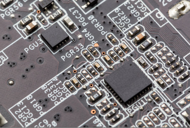
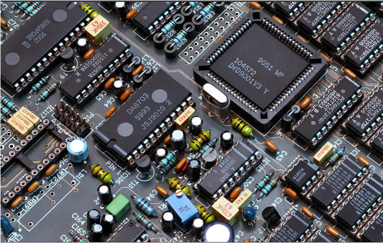
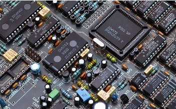
PCBA processing
Advantages of SPI
1. Reduce defects
SPI is first used to reduce defects caused by improper solder paste printing. Therefore, the primary advantage of SPI lies in its ability to reduce defects. As far as SMT assembly is concerned, defects have always been a major problem. The reduction in their number will lay a solid foundation for the high reliability of the product.
2. High efficiency
Think of the traditional SMT assembly process rework model. Unless inspection is performed, that is, usually after reflow soldering, no defects will be exposed. Usually, AOI or X-ray inspection is used to find defects and then rework. If SPI is used, defects can be found at the beginning of the SMT assembly process after the solder paste is printed. Once the incorrect solder paste printing is found, it can be reworked immediately to obtain high-quality PCB solder paste printing. Will save more time and improve manufacturing efficiency.
3. Low cost
For the application of SPI machine, low cost has two meanings. On the one hand, since defects can be found in the early stages of the SMT assembly process, and rework can be completed in time, time costs will be reduced. On the other hand, since defects can be stopped earlier to avoid delaying early defects to the later manufacturing stage, leading to threatening defects, capital will also be reduced.
Fourth, high reliability
Most of the defects in SMT assembly products stem from low-quality PCB solder paste printing. Since SPI is conducive to reducing defects, it will help improve the reliability of PCB products by strictly controlling the source of defects.