The ISO9001-2008 system standard should be strictly implemented in the management and production of the working environment of the SMT placement machine. Introduce foreign advanced "5S" management concepts. Here is a brief share with you on the management specifications of the working environment of SMT placement machines.
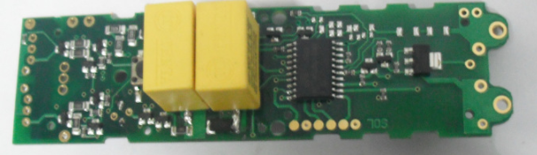
1. SMT patch material management formulates material placement standards, and all materials are placed in areas, racks, and locations according to requirements, and are labeled with corresponding signs. There are corresponding operating specifications for guidance on the acquisition and playback of materials, and corresponding records are made.
2. Environmental management of SMT placement machine production workshop
The production workshop of the SMT placement machine should formulate a production management system, requiring workshop personnel to abide by the process discipline and operate in strict accordance with the operating procedures; require all equipment, articles, raw materials, and tools to be free of dust; stairs and floors are clean and free of garbage; doors and windows are clean and dust-free ; Public passages are unblocked and free of debris; to achieve "one-in-a-day inspection" and "a day-to-day inspection", there are corresponding inspections and records every day.

The cleanliness, temperature and humidity of the SMT placement machine workshop are controlled according to the process documents. The cleanliness of the air in the workshop is 100,000 (BGJ73-84); in an air-conditioned environment, there must be a certain amount of fresh air, and try to control the CO2 content below 1000PPM and the CO content below 10PPM to ensure human health. The best environment temperature of the workshop is 23±3 degree Celsius, the limit temperature is 15~35 degree Celsius; the relative humidity is 45%~70%RH. Add curtains to the windows on the wall to avoid direct sunlight on the equipment. All operations are recorded in the book. Arrange the lighting in the workshop, the illuminance is 800~1200lx. At least not less than 300lx. When the illuminance is low, local lighting should be set.
3. Control of supporting facilities of SMT placement machine
1. SMT placement machine power management and control
The power supply voltage should be stable, generally single-phase AC 220V, three-phase AC 380V. The power supply of the post-installation machine requires independent grounding. Generally, a three-phase five-wire connection method is adopted, and the working zero line of the power supply is strictly separated from the protection line. Install a line filter or AC voltage stabilizer in front of the equipment's transformer.
2. Air source control of SMT placement machine
Configure the pressure of the air source according to the requirements of the equipment. Generally, the pressure is greater than 7KG/cm2. The compressed air shall be introduced into the corresponding equipment of the production line with a uniformly equipped air source network, and the air compressor must be at a certain distance from the SMT production workshop; the compressed air shall be treated with oil removal, dust removal and water removal.
3. Control of the exhaust air volume of the SMT placement machine production line
Both reflow soldering and wave soldering equipment have exhaust air requirements, and exhaust fans are configured according to equipment requirements. The minimum flow value of exhaust ducts for all hot blast stoves is generally controlled at 500 cubic feet per minute.
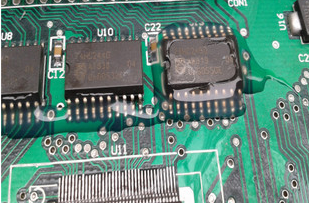
SMT patch technology to reduce voids
There will be voids when welding large flat and low-foot-height components, such as QFN components. The use of these types of components is increasing. In order to meet IPC standards, the formation of voids has caused headaches for many designers, SMD production line operators, and quality control personnel. This article focuses on a new method to reduce voids.
The parameters for optimizing void performance are usually the chemical composition of the solder paste, the reflow temperature profile, the coating of the substrate and components, and the design of the pad and template. However, in practice, there are obvious limitations to changing these parameters. Despite a lot of efforts to optimize, but still often see too high void rate level.
Varying degrees of voids
When we look closely at the solder joints and voids, a major parameter seems to have not attracted people's attention. This is the solder alloy.
As a preliminary test, the three commonly used lead-free solder alloys on the market all have the characteristics of voiding behavior.
Further research strategies include using tin, bismuth, silver, zinc, copper and other elements to adjust these alloys and observe their effects on void behavior. Since this method quickly produced many alloys, TGA analysis was used as an initial selection tool. Using TGA analysis, it is possible to monitor the evaporation and reflow temperature profile of the flux chemical composition in the process of combining with a certain alloy. Experience has shown that a smoother evaporation curve generally means a lower level of void formation. From this study, eight prototype solder alloys were selected and characterized by their void behavior.
To this end, 60 QFNs coated with each alloy were soldered on three different coated substrates: NiAu (ENIG), OSP, and I-Sn. The chemical composition of solder paste, template thickness and layout, and substrate layout used in all alloys are the same. The welding temperature curve is used according to the melting point of the alloy. X-rays are used to determine the void rate level. One of the alloys obtained the best results in cavitation behavior and was selected for further mechanical reliability testing.
Introduction
The mechanism of void formation in solder joints has been the subject of research for many years. Many void types and formation mechanisms have been identified. The most striking thing is the large voids. The main factor in the formation of large voids seems to be the chemical composition in the solder paste.
Microvoids, shrinkage voids and Kirkendall voids are also well-known and well-documented voids
Type, but it is not within the scope of this article. Many techniques for reducing void formation have been established over the years.
Adjusting the chemical composition of solder paste, reflow soldering temperature profile, component, PCB and template design or coating are some optimization tools that are currently being widely used. Even equipment manufacturers are offering solutions to reduce void rates, through frequency sweeping or vacuum technology. However, there is another very important parameter that defines void formation-welding alloys.
Welding alloy: An unusual and suspicious factor. The main cause of void formation has always been considered to be the flux in the solder paste. Designing a solder paste flux that can effectively reduce voids seems to be the correct method, because about 50% of the flux will evaporate during the reflow process, resulting in voids. Since the focus is on the solder paste flux, until now, the research on the difference in void formation of different solder alloys has not paid much attention.
The void level is measured with standard solderable alloys, and a baseline void formation percentage is established, such as SnAg3Cu0.5 (SAC305), SnAg0.3Cu0.7 (LowSAC0307) and Sn42Bi57Ag1. The same solder paste chemistry was used in all the tests described in this article.
In order to understand the level difference between PCB finishes, three kinds of finishes commonly used in the industry were tested:
OSPCu, ENIG (NiAu) and I-Sn. In order to have enough voids, a 120 μm template was used without any reduction in the PCB pad. For each solder paste, 60 Sn-coated QFN components are reflow soldered using a standard heating reflow profile suitable for each specific solder alloy.