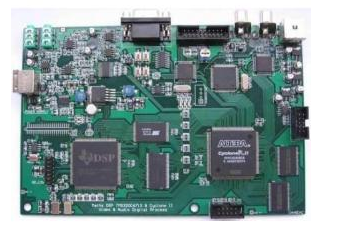
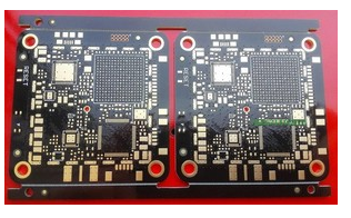
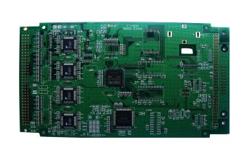
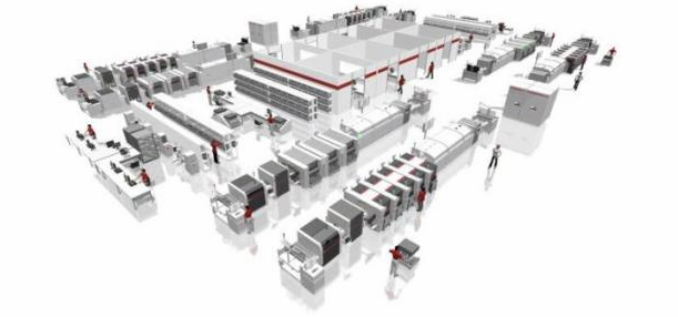
The trend of SMT placement machine
After more than 20 years of development, SMT has now become the main technical means for PCB circuit component-level interconnection of modern electronic works. Relevant data show that the penetration rate of SMT applications in developed countries has exceeded 75%, and it has further developed into the assembly technology field represented by high-density assembly and three-dimensional assembly. The continuous development of assembly technology will inevitably put forward new requirements for the development of assembly technology and related equipment. How to shorten the running time, accelerate the conversion time, and continuously introduce components with a large number of pins and fine pitches has become a severe challenge faced by today's placement equipment. Choosing the appropriate placement equipment to meet the needs of today’s applications is a very difficult decision, but it is a very important choice, because the production capabilities and multi-functional adaptability of electronic works depend on the placement equipment. quite big.
In order to increase production efficiency faster and reduce working time, the new placement machine is developing in the direction of high-efficiency two-way conveying structure.

On the basis of retaining the performance of the traditional single-path placement machine, the dual-path conveyor placement machine designs the PCB transportation, positioning, detection, placement, etc. into a dual-path structure.
In order to enhance adaptability and use efficiency, the new placement machine is developing towards a flexible placement system and a modular structure. The placement machine is divided into a control host and a functional module machine. The module machine has different functions. According to the placement requirements of different components, it can be placed according to different precision and efficiency to achieve higher efficiency; when the user When there are new requirements, new functional modules can be added as needed. Because it can flexibly add different types of placement units according to future needs to meet future flexible production needs, this kind of modular structure machine is very popular with customers. When the work is adjusted, it is very important to be able to improve the work adaptability of the equipment in time. Important, because new packaging and circuit boards have brought new requirements. Investment in a placement equipment should often be based on current considerations and estimates of future needs. Buying a device with much more features than needed today can often avoid business opportunities that may be missed in the future. It is more economically more cost-effective to upgrade on existing equipment than to buy a new one.
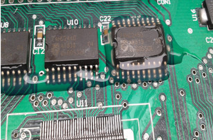
Avoid the disadvantages encountered by solder paste printing during SMT processing
Solder paste printing is a complicated process in SMT patch processing, and it is prone to some shortcomings, which affect the quality of the final product. Therefore, in order to avoid some failures often occur in printing, the common shortcomings of SMT processing solder paste printing can be avoided or solved:
1. Draw the tip. Generally, the solder paste on the pad will be hill-shaped after printing.
Cause: It may be caused by the gap of the squeegee or the viscosity of the solder paste.
Avoidance or solution: SMT chip processing properly adjust the gap of the scraper or select a solder paste with suitable viscosity.
2. The solder paste is too thin.
The reasons for are: 1. The template is too thin; 2. The pressure of the squeegee is too large; 3. The flowability of the solder paste is poor.
Avoidance or solution: choose a template with a suitable thickness; choose a solder paste with suitable granularity and viscosity; reduce the pressure of the squeegee.
3. After printing, the thickness of the solder paste on the PCB pads varies.
Reasons: 1. The solder paste is not uniformly mixed, so that the particle size is not common. 2. The template is not parallel to the printed board;
Avoidance or solution: Fully mix the solder paste before printing; adjust the relative position of the template and the printed board.
Fourth, the thickness is not the same, there are burrs on the edges and appearance.
Reasons: It may be that the viscosity of the solder paste is low, and the wall of the template hole is rough.
Avoidance or solution: choose a solder paste with a slightly higher viscosity; check the etching quality of the template opening before printing.
Five, fall. After printing, the solder paste sinks to both ends of the pad.
Reasons: 1. The pressure of the squeegee is too large; 2. The positioning of the printed board is not firm; 3. The viscosity of the solder paste or the metal content is too low.
Avoidance or solution: adjust the pressure; fix the printed board from the beginning; select the solder paste with suitable viscosity.
6. Incomplete printing means that solder paste is not printed on some places on the PCB pads.
The reasons are: 1. The hole is blocked or some solder paste sticks to the bottom of the template; 2. The viscosity of the solder paste is too small; 3. There are large-scale metal powder particles in the solder paste; 4. The scraper is worn.
Avoidance or solution: clean the opening and the bottom of the template; select a solder paste with suitable viscosity, and make the solder paste printing can effectively cover the entire printing area; select the solder paste with the metal powder particle size corresponding to the opening size; check and replace the squeegee .