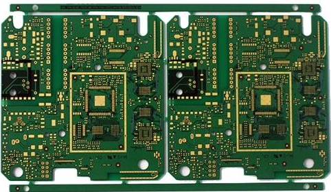
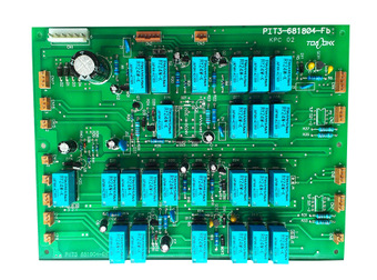
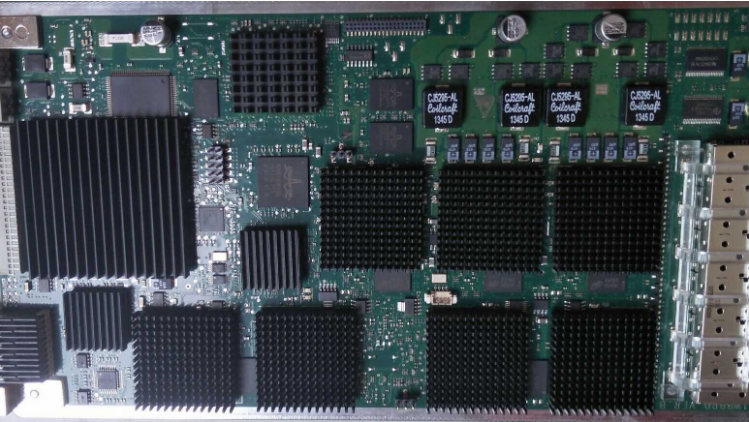
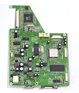
Prevent OEM bad phenomena in SMT foundry production
Some common undesirable phenomena will appear in the OEM produced by smt. Those problems affect the quality of the processed products of the SMT chip processing plant. Then how should those undesirable phenomena in electronic processing be prevented?
1. Poor wetting
Poor wetting refers to the fact that the solder and the soldering area of the substrate during the soldering process do not generate a metal-to-metal reaction after wetting, resulting in missed soldering or less soldering failures.
Solution: Choose a suitable soldering process, take anti-fouling measures on the surface of the substrate and components, choose a suitable solder, and set a reasonable soldering temperature and time.
Two, bridging
Most of the causes of bridging in smt foundry production are due to excessive solder or severe edge collapse after solder printing, or the size of the substrate solder area is out of tolerance, mounting offset, etc., and the circuit tends to be miniaturized., The bridging will cause electrical short circuit and affect the use of the product.

solution:
1. It is necessary to prevent bad edge collapse during solder paste printing.
2. Pay attention to the design requirements of OEM processing when designing the size of the PCBA substrate welding area.
3. The component mounting position should be within the specified range.
4. The wiring gap of PCBA substrate and the coating accuracy of solder resist must be strictly required.
5. Formulate appropriate welding process parameters.
Three, cracks
When the soldered PCB just leaves the solder zone, due to the difference in thermal expansion between the solder and the joined parts, under the action of rapid cold or rapid heat, due to the effect of solidification stress or shrinkage stress, the SMD will basically produce microcracks. During punching and transportation, the impact stress and bending stress on SMD must also be reduced.
Solution: When designing surface mount products, we should consider narrowing the gap in thermal expansion and correctly set heating and cooling conditions. Use solder with good ductility.
Four, solder ball
The production of solder balls mostly occurs when the solder is scattered due to the rapid heating during the soldering process of Shenzhen smt's foundry production. In addition, it is also related to undesirable phenomena such as misalignment, sagging, and pollution of the solder.
solution:
1. To prevent over-rapid and defective welding and heating.
2. Prevent defective products such as solder sag and misalignment.
3. The use of solder paste must comply with SMT processing requirements.
4. Implement the corresponding preheating process according to the welding type.
Principle and application of X-ray detection
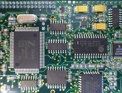
With the continuous development of electronic technology, SMT technology has become more and more popular, the size of single-chip microcomputer chips has also become smaller and smaller, and the pins of single-chip microcomputer chips have gradually increased, especially the BGA single-chip microcomputer chips that have appeared in recent years. Because the pins of the BGA single-chip microcomputer chip are not distributed around according to the traditional design, but are distributed on the bottom surface of the single-chip microcomputer chip, it is undoubtedly impossible to judge the quality of the solder joints according to the traditional manual visual inspection. It must be based on ICT and even functional testing. But under normal circumstances, if there are batch errors, they cannot be found and corrected in time, and manual visual inspection is the most inaccurate and reproducible technology, so X-ray inspection technology is becoming more and more widely used in SMT reflow In post-welding inspection, it can not only perform qualitative and quantitative analysis on the solder joints, but also find faults in time and make corrections.
1. The working principle of X-ray machine:
When the board enters the inside of the machine along the guide rails, there is an X-ray emission tube above the board. The X-ray emitted by the board passes through the board and is received by the detector (usually a camera) placed below. The lead that absorbs X-rays, so compared with the X-rays that pass through glass fiber copper, silicon and other materials, the X-rays irradiated on the solder joints are absorbed a lot, and the appearance of black spots produces a good image, which makes the solder joints The analysis becomes quite simple and intuitive, so a simple image analysis algorithm can automatically and reliably detect solder joint defects.
2. X-ray technology:
X-ray technology has evolved from the previous 2D inspection method station to the current 3D inspection method. The former is a projected X-ray inspection method, which can produce clear visual images for the period solder joints on a single panel, but for the currently widely used double The effect of surface reflow soldering board is very poor, which makes the visual images of the solder joints on both sides overlap and is extremely difficult to distinguish. However, the latter 3D inspection method uses layering technology, which focuses the beam on any layer and projects the corresponding image to a high-speed On the rotating receiving surface, because the receiving surface tells the rotation to make the image at the intersection point very clear, while the images on other layers are eliminated, the 3D inspection method can independently image the solder joints on both sides of the board.
In addition to the detection of double-sided soldering boards, 3DX-ray technology can also perform multi-layer image slice detection on invisible solder joints such as BGA, that is, thoroughly detect the top, middle, and bottom of the BGA solder ball joints, and use This method can also measure through-hole PTH solder joints to check whether the solder in the through-hole is sufficient, thereby greatly improving the connection quality of the solder joints.
3. X-ray replaces ICT
As the density of printing plates becomes higher and higher, SMT devices become smaller and smaller, and the point space left for ICT testing in the design of printed boards becomes smaller and smaller, or even cancelled. In addition, for complex printing If the board is directly sent from the SMT production line to the functional test position, it will not only lead to a decline in the pass rate, but also increase the board’s fault diagnosis and repair costs, and even cause delivery delays, and lose its competitiveness in today's fiercely competitive market. If X-ray inspection is used instead of ICT at this time, it can ensure the production path of functional testing, reduce fault diagnosis and repair work. In addition, by using X-ray for spot inspection in SMT production, batch errors can be reduced or even eliminated. It is worth noting that for those solders that cannot be detected by ICT, there is too little or too much solder, and X-rays such as cold sweat, soldering or pores can also be measured, and such defects can easily pass ICT and even functional tests without being found, so Affect the product life. Of course, X-ray cannot detect the electrical defects of the device, but these can be detected in the functional test. In short, the addition of X-ray detection will not only miss any defects in the manufacturing process, but can also detect Some shortcomings that ICT can't find.
Based on the above factors, the 3DX-ray machine can evaluate the size, shape and characteristics of each SMT solder joint, and automatically detect unacceptable and critical solder joints. Critical solder joints are solder joints that will cause premature product failure. Of course These critical solder joints will be considered good solder joints in other tests.