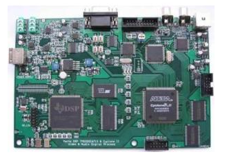
Have you ever wondered how the vision and robotic system in a surface mount SMT placement machine (SMT) can accurately place electronic components in the required positions on a tiny printed circuit board with very small tolerances?
The goals of the SMT vision system are diverse: match the circuit pattern of the artwork with the top or bottom of the manufactured printed circuit board (PCB), determine the position of the PCB on the x, y, and z planes, and on the circuit Position the precise location to place specific components. With the help of the indexing (positioning) system, the PCB is positioned according to the program parameters, but this positioning is not accurate enough for component placement. The silk screen provides a reference point for the imaging system.
What is silk screen?
Although it sounds like a financial term, the term "benchmark" refers to a fixed reference basis for comparison purposes. Generally, silk screens are embedded object or surface markings that are used as a directional measurement or reference point for indexing and imaging systems.

Silk screen is used in multiple industries and applications, such as physics, 3D computer graphics, optics and photography. They are used in geophysical flight to refer to measurement results, in augmented reality media to locate the position of activated composite images or game boards, and in medical imaging by correlating body scans with body positions.
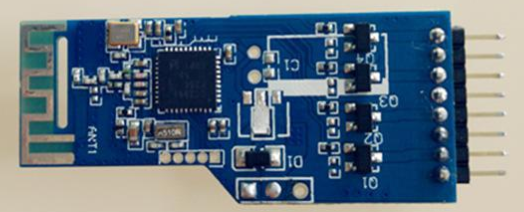
In automated electronic assembly applications, silk screen is an alignment mark used in the indexing system to make the PCB oriented in the correct direction and skewed. The vision system uses silk screen placement to accurately insert components into the circuit. Silk screen, also known as "circuit pattern recognition mark", is a key aspect of testing and packaging throughout the entire automated manufacturing process. The importance of silk screen placement cannot be underestimated, because if the exact position of the PCB circuit board or circuit cannot be measured correctly at any time during the assembly process, an automated "train wreck" will appear!
How does the placement of the silk screen affect the insertion of components?
Precise silkscreen placement ensures that your PCB faces the correct direction and is aligned as close as possible to perfection. The SMT placement machine uses the camera to locate the silk screen, and then adjusts the position of the components according to the exact position of the circuit board.
The disadvantage of robotic assembly arms is that they won't complain to you about how long the working hours are.
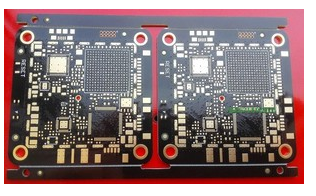
The PCB is delivered to the SMT machine for assembly from the conveyor belt. The fixing or clamping direction of each PCB is slightly different from other PCBs, and this small change is enough to destroy the circuit board unless it is recalibrated. To this end, two or three fiducials are marked on the PCB so that the placement robot can accurately determine the direction of the circuit board. By comparing the actual position of the silk screen relative to the plan view of the circuit board stored in the machine's memory, the vision system can reliably calculate the "offset" to which the part must be moved in order to accurately place the part.
How to set the silk screen on the printed circuit board?
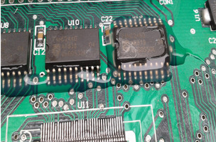
Silk screen is usually made by making the circular area of the printed circuit board not covered by the solder mask. In this circular area, the underlying copper plating is exposed. Good image recognition requires nothing around the silk screen, so when assembling, you must pay attention to the "matt" background around the silk screen. Alternatively, a transparent solder mask can be used to cover the fiducials because the vision system can still detect the copper ring.
From the first two reference points (placed diagonally to each other), the machine can identify the position of the PCB and the inclination of the PCB in the transfer clamp through its X and Y positions. Finally, the third benchmark can help the machine compensate for any shrinkage or stretching of the PCB.
If the components are placed on a double-sided PCB design, reference points must be placed on both sides of the PCB. The placement of multiple silk screens for PCB positioning is called a "global datum". Components that require high positioning accuracy may have a single "local datum" placed near the component location to provide higher accuracy.
What will happen if silk screen is not used?
If you manually assemble a single or prototype board, it is okay not to use silk screen. However, if you plan to automate production, then you will find that SMT placement machines will not be an option because their operation requires reference points on the PCB to align them correctly. In addition, manual assembly will result in a higher percentage of boards failing testing and quality standards, and it will take a lot of time to repair imperfect manual welding.
Tips for silk screen placement:
SMT chip processing plant: The following are some tips for placing silk screens on printed circuit boards:
1. The best size of silk screen should be between 1mm and 3mm. Aim for a matt "buffer" area that is roughly the same size as the diameter of the mark around the mark.
2. The silk screen must have no solder mask, unless the cover is transparent.
3. For the overall reference, there should be at least 2 marks, preferably 3 marks to ensure the accuracy of component placement. The marks should be located on opposite ends of each other and separated as much as possible on the board. If you have 3 silk screens, please place them in a triangle and keep the space as wide as possible on the board.
4. If there is not enough space on the edge of the circuit board, a global silk screen is required.
5. The distance from the silk screen to the edge of the board should be 0.3 inches, excluding the silk screen buffer area.
6. For local fiducial points, place at least two silk screens diagonally on the outer edge around the specific component. In order to correct placement errors on the components, local silk screens can also be used.
7. The placement of silk screens can make a smooth assembly line different from an assembly line that continuously needs adjustment. Even if the supplier tells you that they have upgraded the machine to work without marking, it is wise to always incorporate silk screen into the circuit board design. You may need these marks during testing or when you may need to rework in the future.