Key points:
· Understand ground and voltage routing across printed circuit board layout and design
· Best practices for implementing power and ground planes in PCB design
It is very easy to plug the power cord into the wall socket or turn on the light switch. You might think that it is also easy to connect the components on the printed circuit board to the power source or ground. To be honest, this was once the case with PCB design. On boards where signal and power integrity are not very important, you can place vias in the power or ground plane and ignore them.
However, according to the design requirements of today's electronic products, there are many things to manage the power distribution network, not just add some vias in the design. You need to consider the impact of the PDN on the rest of the circuit board, while still ensuring that the equipment can use the proper power and ground grids. This requires some skill in the grounding and voltage wiring of your circuit board, and we provide some useful ideas here.
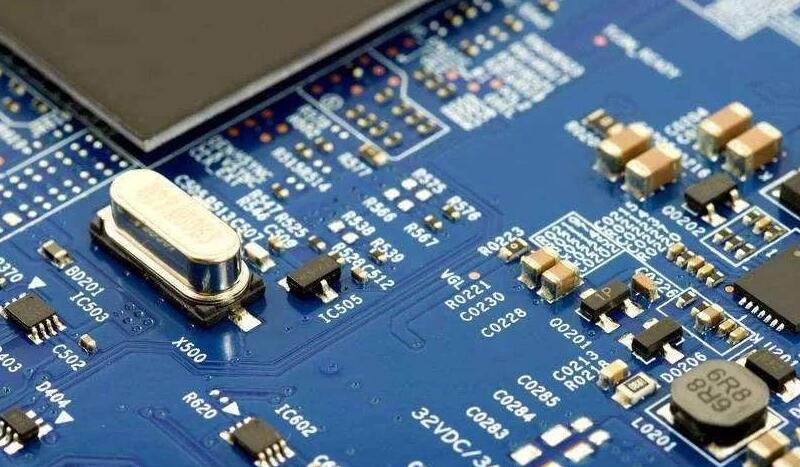
Ground and voltage wiring on the printed circuit board

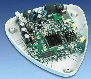
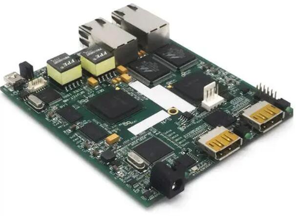
Although today's dense multi-layer boards are widely used in advanced electronic equipment, there is still a need for cheap two-layer boards. For devices that do not require many circuits (such as toys or other simple consumer products), two-layer boards are still preferred to reduce manufacturing time and costs. However, at the same time, the performance of these electronic devices is still improving, which requires more efforts in the design of the power supply network of the circuit board.
Only two layers are required for use, and there are no internal layers available for the power and ground planes, so you will have to route the power. It is recommended that in most applications, designers use the smallest possible trace width and still can be manufactured at a low price. Usually this ends up with 6 million traces of the signal and 20 million traces of the power. Remember that the power trace width is proportional to the current-if the current increases, the trace width will increase, and vice versa.
When routing, signal and power routing should be placed on the top layer, and the return path should be reserved on the bottom layer. The easiest way is to dedicate the bottom layer as a solid ground plane. You may end up having to use some of the underlying layers for signal routing, but if you want to make sure to maintain a clear path for the signal return.
Routing voltage and signal routing requires careful planning
Using a bottom ground can also help you solve noise and other signal integrity issues, but it will also take up a lot of space. Therefore, it is important to carefully plan the top-level power supply wiring to ensure that the power supply is evenly distributed across the board.
If the SMT pin is connected to a power supply or ground with a large area of metal, it may cause a thermal imbalance between the SMT pin and the pin with less metal. In smaller discrete parts with two legs, this imbalance can cause a condition called "tombstone strike". This is where the solder reflow rate on one pin is faster than the other pin, and the part is pulled up and away from the other pin.
When connecting discrete SMT pins to ground or voltage wiring, it is best to use a trace width that is wide enough to meet the current demand to provide heat dissipation. This will help keep the two pins of the device thermally balanced.
Another problem with small discrete parts is to place a pin on a large area of metal. Although this provides the best electrical performance, it also acts as a huge heat sink, creating a large thermal imbalance with the other pin. The best practice to meet electrical design and PCB manufacturing needs is to connect SMT pins to multiple traces or "connections." This provides the heat dissipation required for soldering to the SMT pins.
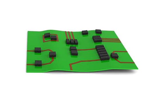
Through hole pin:
The connection of through-hole pins to power and ground traces is usually the same as any other trace, requiring direct connection from the trace to the pad of the pin. If the trace is wider than the pad, or there is a metal-filled area (such as a power or ground plane), you need to use a thermal pad, as shown in the figure below.
These heat sinks can provide a sufficient amount of metal to conduct current, but will reduce the heat drawn from the pins by the metal plane. With a PCB design tool such as Cadence Allegro, you can control the width of the cable tie and spacing in the thermal pad to provide enough metal for the pad to meet its needs.
The heat sink of the through-hole pin in the ground plane
Advantages and disadvantages of power supply and ground plane
If you want to design a multi-layer circuit board, you may need to configure a board stack for dedicated power and ground planes. The biggest advantage of using an airplane is that it provides an easy way to connect components to the power supply and the ground without the need for wide traces and wiring like on a two-layer board. Using a ground plane in your design can also bring you many other benefits, including:
· Return path: The signal will travel from its source to its destination, and then needs to return to its source. If there is no clear return path, they will produce a lot of noise when hovering around, which may affect other circuits. The ground plane will provide this simple return path.
· Shielding: The grounding layer will help shield sensitive circuits from external electromagnetic interference (EMI) and prevent the internally generated EMI from affecting other equipment. In addition, the use of ground planes between active signal layers in the design will help reduce the possibility of broadside coupling or crosstalk between the layers.
· Reduce noise: When the digital circuit switches states, it will generate noise pulses through the ground circuit, which may cause false switching in other circuits. The large area of the ground plane will help reduce the impact because its impedance is lower than the impedance of the ground wire through the trace.
· Heat dissipation: The ground plane also provides a good heat sink for components that run hot. By connecting these parts with holes to the ground plane through the circuit board, the heat can be evenly distributed on the circuit board.
· On the other hand, there are some shortcomings to be aware of when using power and ground planes. The plane will increase the number of layers of the board, which will increase the manufacturing cost. Different areas of the circuit (such as digital and analog) will need to carefully manage their grounding so that noise from one circuit does not adversely affect the other circuit. And, when using a split aircraft to accommodate multiple power sources or grounding grids, extreme care must be taken. This is especially important for the signal return path, because the separation plane may inadvertently destroy or block paths that should be unobstructed.
However, all these problems are part of the PCB design process, and advanced PCB design tools can be used to skillfully solve these problems.