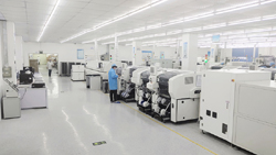
AOI, also known as automatic optical inspection instrument, is an automatic optical inspection device applied to the surface mount production line, which can effectively detect the quality of printing, mounting and solder joints. The core of AOI is the CCD camera system to capture pictures, but after processing by a series of algorithms such as image processing cards and computer processing software systems, they are compared with standard images, defects are found, and documents are produced. Using AOI can find and eliminate errors in the early stage of the assembly process to achieve good process control. Early detection of defects will avoid sending defective products to the assembly stage of the subsequent process, and AOI will reduce repair costs and avoid scrapping unrepairable PCB circuit boards.

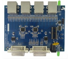
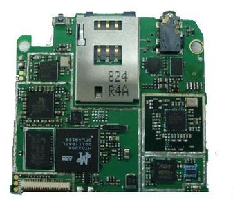
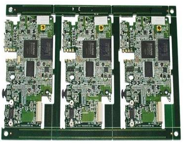
Printed circuit boards (PCBs for short) are substrates for assembling electronic parts, and the manufacturing quality of PCB boards directly affects the reliability of electronic products. With the in-depth development of electronic assembly to higher density and smaller size PCB hybrid technology, in order to reduce the number of defective circuit boards entering the next step, the demand for automatic optical inspection (AOI) systems for PCB inspection is also increasing. Big.
The AOI system has incomparable technical advantages over other inspection schemes and traditional inspection methods, and has been widely used in PCB inspection. Its high-speed, high-school and high-precision functional characteristics are favored by industry users.
1. The PCB inspection system checks and corrects PCB defects, and the cost during the process monitoring is much lower than the cost after the final test and inspection.
2. Repetitive errors can be found as early as possible, such as placement displacement or incorrect tray installation.
3. The combination of the statistical analysis function of the PCB inspection technology and the SPC process management technology provides a powerful weapon for the timely improvement of the SMT production process, and the yield of PCB assembly has been significantly improved. With the continuous expansion of the scale of modern manufacturing, the control of production is becoming more and more important, and the demand for SPC data is also increasing.
4. It can meet the testing requirements of PCB assembly density. With the substantial increase in the assembly density of electronic products, some traditional testing technologies, such as ICT, can no longer meet the development requirements of SMT technology, and PCB testing technology will not be affected by these factors.
5. The test program of PCB testing equipment can be directly generated from CAD data. Compared with ICT, since no special fixture is required, the test cost is also greatly reduced.
6. It can keep up with the production cycle of the SMT production line. According to the test results of PCB inspection technology, it can achieve a speed of 0.1 second/frame at present, which can meet the requirements of online inspection.
7. High reliability of detection Manual visual inspection always has its limitations, while PCB inspection technology testing avoids disadvantages in this regard, and can maintain better accuracy and reliability.