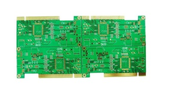
The selection and design of surface-mounted components is a key part of the overall product design. The designer determines the electrical performance and function of the components in the system structure and detailed circuit design stage. In the SMT design stage, it should be based on the specific conditions and overall situation of the equipment and process. The design requirements determine the packaging form and structure of surface mount components. Surface-mounted solder joints are both mechanical connection points and electrical connection points. A reasonable choice will have a decisive impact on improving PCB design density, productivity, testability and reliability.
There is no difference in function between surface mount components and plug-in components. The difference lies in the packaging of the components. Surface-mounted packages must withstand high milk temperatures during soldering,

and their components and substrates must have matching thermal expansion coefficients. These factors must be fully considered in product design.
The main advantages of choosing the right package are:
1). Effectively save PCB area;
2). Provide better electrical performance;
3). Protect the interior of the components from environmental influences such as humidity;
4). Provide good communication links;
5). Help dissipate heat and provide convenience for transmission and testing.
Selection of surface mount components
Surface mount components are divided into two categories: active and passive. According to the shape of the pin, it is divided into gull wing type and "J" type. The following describes the selection of components in this category.
Passive components
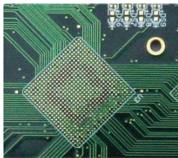
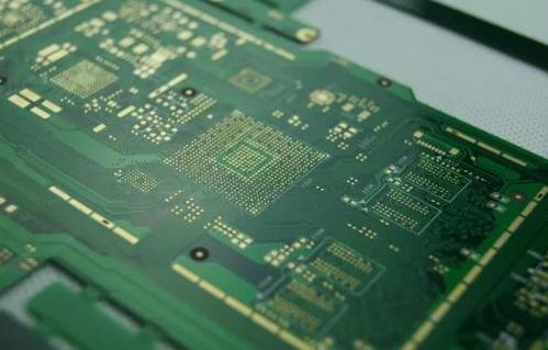
Passive devices mainly include monolithic ceramic capacitors, tantalum capacitors, and thick film resistors, with a rectangular or cylindrical shape. Cylindrical passive components are called "MELF". They are prone to rolling when reflow soldering. Special pad design is required and should generally be avoided. Rectangular passive components are called "CHIP" chip components. They are small in size, light in weight, antimicrobial impact and shock resistance, and low parasitic loss. They are widely used in various electronic products. In order to obtain good solderability, the electroplating of the nickel barrier layer must be selected.
Active device
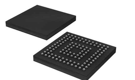
There are two main types of surface mount chip carriers: ceramics and plastics.
The advantages of ceramic chip packaging are: 1) Good airtightness and good protection for the internal structure 2) Short signal path, significantly improved parasitic parameters, noise, and delay characteristics 3) Reduce power consumption. The disadvantage is that because the leadless absorbs the stress generated when the solder paste melts, the CTE mismatch between the package and the substrate can cause solder joints to crack during soldering. The most commonly used ceramic wafer carrier is the leadless ceramic wafer carrier LCCC.
Plastic packaging is widely used in the production of military and civilian products, and has a good cost performance. Its packaging forms are divided into: small outline transistor SOT; small outline integrated circuit SOIC; plastic package leaded chip carrier PLCC; small outline J package; plastic flat package PQFP.
In order to effectively reduce the area of the PCB circuit board, SOIC with a pin count of less than 20, PLCC with a pin count between 20-84, and a PQFP with a pin count greater than 84 are preferred when the device functions and performance are the same.