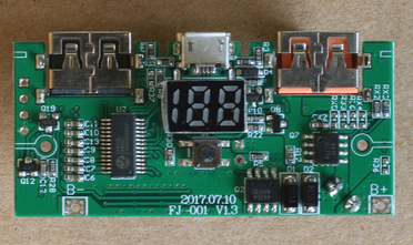
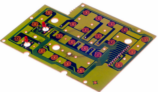
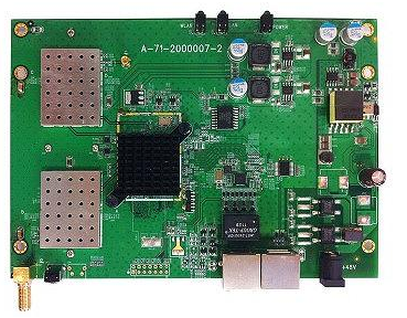
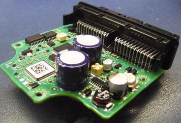
What are the design processes for SMT patch printed circuit boards
1. Design the electrical schematic diagram
The main work of designing the electrical schematic diagram is to use the software to draw the schematic diagram of the circuit, and compile and generate the network table.
What are the design processes for SMT patch printed circuit boards
2. Create a PCB document
Through the creation of PCB documents, the PCB editor is called up, and the design work is completed in the PCB editing environment.
What are the design processes for SMT patch printed circuit boards
3. Planning the circuit board
Before drawing the printed circuit board diagram, the designer should also plan the circuit board, including defining the size and shape of the circuit board, setting the layer of the circuit board and setting parameters. This is an extremely important task and a basic framework for circuit board design.
What are the design processes for SMT patch printed circuit boards

4. Load component package library and netlist
To place the components on the printed circuit board, you need to load the package library of the used components first, otherwise the component package cannot be called out when importing the schematic information to the PCB, resulting in errors.
What are the design processes for SMT patch printed circuit boards
5. Component layout
The layout is to place the components in the proper position on the printed board. The "appropriate location" here has two meanings. One is that the location of the component can make the entire circuit board meet the requirements of electrical signal flow design and anti-interference, and it looks neat and beautiful; the other is that the location of the component is conducive to wiring .
What are the design processes for SMT patch printed circuit boards
6. Set wiring rules
For components and network labels with special requirements, it is generally necessary to set wiring rules before wiring, such as safety spacing, wire width, wiring layer, etc.
What are the design processes for SMT patch printed circuit boards
7. Wiring
Wiring is to lay copper wires to realize the electrical connection between the various pads. This operation can be done either automatically or manually. Altium Designer 10's automatic routing function is very powerful. If the component layout is reasonable and the routing rules are set properly, the success rate of automatic routing is close to 100%; if the automatic routing cannot be completely resolved or a routing conflict occurs, It can be adjusted by manual wiring.
What are the design processes for SMT patch printed circuit boards
8. Generate reports and print out
After completing the wiring of the circuit board, save the PCB diagram, and then use various graphics output devices to output the PCB diagram. After the PCB diagram is designed according to the above process, the document can be handed over to the printed circuit board production unit for production.
The above is about the SMT chip printed circuit board design process, I hope it will be helpful to everyone.