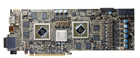
With the rapid development of modern electronic technology, PCBA is also developing towards high density and high reliability. Although the current PCB and PCBA manufacturing technology level has been greatly improved, the conventional PCB welding process will not be fatal to the product manufacturability. However, for devices with very small pin spacing, the unreasonable design of PCB welding pad and PCB blocking pad will increase the difficulty of SMT welding process and increase the quality risk of PCBA surface mount processing. In view of the potential manufacturability and reliability problems caused by the unreasonable design of PCB welding pad and blocking pad, the manufacturability problems can be avoided by optimizing the device packaging design based on the actual process level of PCB and PCBA. Optimization design mainly from two aspects, first, PCB LAYOUT optimization design; Second, PCB engineering optimization design.

PCB resistance welding design status
Research on manufacturability of PCBA by PCB resistance welding design
PCB layout design
Package design according to IPC 7351 standard package library and refer to the pad size recommended in the device specification. For rapid design, Layout engineers should increase the size of the pad according to the recommended size to modify the design. The length and width of PCB welding pad should be increased by 0.1mm, and the length and width of block welding pad should be increased by 0.1mm on the basis of the welding pad.
What is the impact of PCB welding design neglect on PCBA manufacturing process
PCB Engineering Design
Conventional PCB blocking welding process requires that the edge of the pad should be covered by 0.05mm, and the middle blocking bridge of the two pads should be larger than 0.1mm. In the design stage of PCB engineering, when the size of the pad cannot be optimized and the middle blocking bridge of the two pads is smaller than 0.1mm, the group blocking plate window design is adopted for PCB engineering.
What is the impact of PCB welding design neglect on PCBA manufacturing process
PCB resistance welding design requirements
Research on manufacturability of PCBA by PCB resistance welding design
PCB layout design requirements
When the two pad edge spacing greater than 0.2mm pad, according to the conventional pad packaging design; When the distance between the edges of the two pads is less than 0.2mm, the DFM optimization design is needed. The DFM optimization design method is helpful for the optimization of the size of the pads. Ensure that solder blocking agent in solder blocking process can form solder bridge isolation pad during PCB manufacturing.
PCB engineering design requirements
When the edge distance between the two pads is greater than 0.2mm, the engineering design shall be carried out according to the conventional requirements; When the distance between the edges of two pads is less than 0.2mm, DFM design is needed. The DFM method of engineering design includes design optimization of welding resistance layer and copper cutting of welding aid layer. The size of copper-cutting must refer to the device specification. The copper-cutting pad should be within the size range of the recommended pad design, and the PCB blocking welding design should be single-pad window design, that is, the blocking bridge can be covered between the pads. Ensure that in PCBA manufacturing process, there is a blocking welding bridge between the two pads for isolation, to avoid welding appearance quality problems and electrical performance reliability problems.
PCBA process capability requirements
Research on manufacturability of PCBA by PCB resistance welding design
Welding resistance film in the process of welding assembly can effectively prevent welding bridge short connection, for high-density PCB with fine spacing pins, if the open welding bridge between the pins is isolated, PCBA processing plant can not guarantee the local welding quality of the product. For PCB isolated by open welding of high-density and fine spacing pins, the current PCBA manufacturing factory determines that the incoming material of PCB is defective and does not allow online production. In order to avoid quality risks, PCBA manufacturing factory will not guarantee the welding quality of products if the customer insists on putting the products online. It is predicted that welding quality problems in the manufacturing process of PCBA factory will be dealt with through negotiation.
Analysis of the
Research on manufacturability of PCBA by PCB resistance welding design
Device specification book size
As shown in Figure 4, the device pin center spacing: 0.65mm, pin width: 0.2 ~ 0.4mm, pin length: 0.3 ~ 0.5mm.
PCB layout actual design
The size of solder pad is 0.8 * 0.5mm, the size of solder pad is 0.9 * 0.6mm, the center spacing of the device pad is 0.65mm, the edge spacing of solder pad is 0.15mm, the edge spacing of solder pad is 0.05mm, and the width of unilateral solder pad is increased by 0.05mm.
PCB engineering design requirements
According to the conventional welding engineering design, the size of unilateral welding pad should be larger than the size of welding pad 0.05mm, otherwise there will be the risk of welding flux covering the welding pad. As shown in Figure 5, the width of unilateral welding is 0.05mm, which meets the requirements of welding production and processing. However, the distance between the edges of the two pads is only 0.05mm, which does not meet the technological requirements of the bridge. Engineering design directly design the whole row of chip pin design for group welding plate window design.