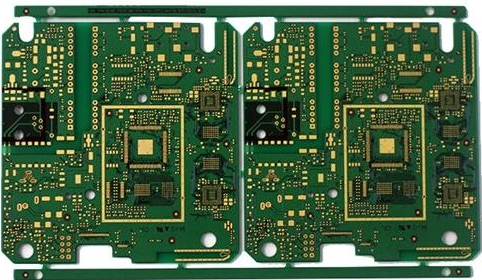
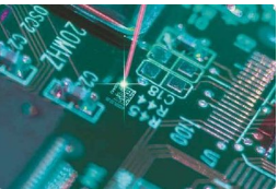
People in the electronics industry involved in the SMT patch proofing process are very important. Printed circuit boards, printed circuit boards, are very widely used as the basis of electronic circuits. Printed circuit boards are used to provide a mechanical basis on which circuits can be built. So almost all the printed circuit boards used in circuits and their designs are used in millions.
Although PCBs today form the basis of almost all electronic circuits, they are often taken for granted. However, the technology is advancing in this regard. Track size is reduced, the number of layers in the board is increasing to accommodate the increased connectivity required, and design rules are improving to ensure that smaller SMT devices can be handled and the soldering process used in production can be accommodated.
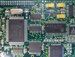
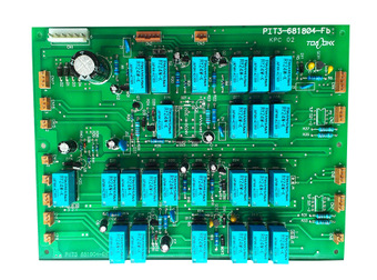
Process requirements for SMT patch proofing

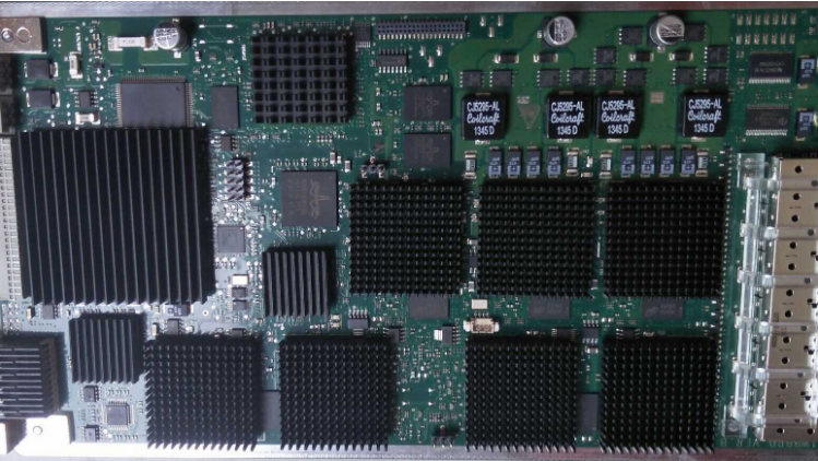
Process requirements for SMT patch proofing and placement of components. Mounted components should be accurately placed one by one on the printed circuit board in accordance with the requirements of the assembly drawing and schedule of the assembly board. 1. SMT processing and placement process requirements. The type, model, nominal value and polarity of each assembly number component on the circuit board must comply with the requirements of the product assembly drawing and schedule.
The mounted components must be intact.
The solder ends or pins of smt chip mount components are not less than 1/2 thickness immersed in solder paste. For general components, the amount of solder paste extrusion should be less than 0.2mm during placement, and for fine-pitch components, the amount of solder paste extrusion should be less than 0.1mm during placement.
The solder ends or pins of the components should be aligned and centered with the land pattern. Due to the self-alignment effect of reflow soldering, a certain deviation is allowed during component mounting. For the specific deviation range of various components, please refer to the relevant IPC standards.
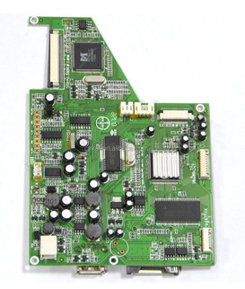
The PCB manufacturing process can be implemented in various ways and has many variations. Despite many small changes, the main stages in the manufacturing process of SMT patch proofing are the same.
Printed circuit boards, printed circuit boards, can be made from a variety of different substances. The most widely used form of glass fiber substrate called FR4. This provides a reasonable degree of stability under temperature changes and is not as severe as the breakdown, although not being overly expensive. Other less expensive materials can be used for printed circuit boards in low-cost commercial products. For high-performance RF designs, the dielectric constant of the substrate is important, and a low level of loss is required, and then PTFE-based printed circuit boards can be used, although they are more difficult to handle.
In order to make the tracks with the components in the PCB, first obtain the copper clad board. This includes the substrate material, usually FR4, and the usual copper cladding on both sides. The copper coating is connected to a thin layer of copper on the motherboard. This combination is usually very good for FR4, but the nature of PTFE makes this more difficult, which increases the difficulty of PTFE PCB processing.