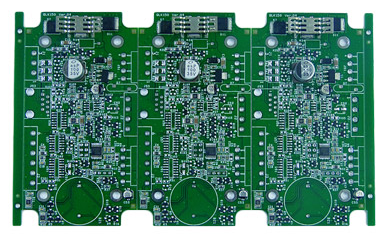
About PCBA factory automatic optical detector
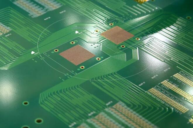
With the reduction of component package size and the increase of printed circuit board patch density, SMA inspection becomes more and more difficult, and manual visual inspection becomes insufficient, and its stability and reliability are difficult to meet the needs of production and quality control. Therefore, it is more and more important to use special inspection equipment to realize automatic inspection. First of all, the inspection instrument used in production is an optical system. This type of instrument has a common feature, that is, the SMA is illuminated by a light source, the reflected light of the SMA is collected by an optical lens for calculation, and the computer image processing system is used to determine whether the SMA is on. Component location and welding conditions, so this type of equipment is called automatic optical inspection (AOI) equipment.
1. AOI working principle
The basic principle of AOI detection is to illuminate the test object through artificial light source, LED light, optical lens and CCD, and compare, analyze and judge the amount of light reflected back with the programmed standard. This section takes AOI after reflow soldering as an example. AOI after reflow is usually divided into two-dimensional AOI and three-dimensional AOI.
Two-dimensional AOI adopts a vertical camera, and realizes the judgment of the quality of solder joints through the color and high-brightness method. The typical product is Omron VT-WIN, as shown in Figure 6-10. When the machine is working, the red, green, and blue ring illuminations are at different heights to illuminate the circuit board. The color camera is installed vertically on the center line of the ring illumination to extract the circuit board image, as shown in Figure 6-11. . Since the red light is located at a higher position from the substrate surface than the other two light rays, the incident angle relative to the substrate surface is larger. The light shining on the flat surface is reflected in the direction of the camera directly above, while the light shining on the solder surface is not reflected directly above. Therefore, for the flat surface part, the camera captures the red area. Similar to the principle of red light, the green area is the slightly inclined solder surface captured by the camera, and the blue area is the steeply inclined solder surface captured by the camera. In this way, the shape of the three-dimensional solder joint can be converted into a two-dimensional color image through the color brightness mode, which can be further processed through image processing combined with a certain mathematical model to achieve the inspection of the quality of the solder joint.

Three-dimensional AOI uses a vertical camera while adding an angle camera. When the vertical camera looks from the top down, the angle camera observes the solder joint image from the side at the same time, just like manual visual inspection. In order to see the local details, it is often necessary to adjust the light and the viewing angle. Therefore, 3D AOI has stronger fault detection capabilities. For example, when testing the welding quality of PLCC devices, the advantages of 3D AOI can be fully revealed. The lighting system in the three-dimensional AOI uses an independently controllable array of light-emitting diodes as the light source. The light-emitting diodes are arranged in a precise ring array, all focused on the field of view. The closer to the inner circle, the closer the light is to the vertical angle, and the closer to the outer circle, the more inclined the illumination angle will be. These diodes can be controlled by programming to achieve the optimal lighting texture, angle, direction and density; it can be used for each inspection screen Adjust the angle, direction and brightness of the illumination to meet the unique requirements of any inspection. Teradyne Optima 7300 AOI is a typical three-dimensional AOI, this model uses a vertical camera and 4 angle cameras to form a detection system.
LED lighting patch processing 008
2. Analysis algorithm
Different A0I software and hardware designs have their own characteristics. In general, the analysis and judgment algorithms can be divided into two types, namely, the design rule check (DRC) method and the pattern recognition method.
The DRC method is to inspect patterns according to some given rules. For example, all connections should be based on solder joints, and all lead widths and intervals are not less than a specified value. Based on the solder paste bridge detection image of the algorithm, after extracting the digital image of the PCB board solder paste, it is judged whether it is a bridge according to the shape of the solder paste in the inter-pad area. If the shape of the solder paste measured at a certain sensitivity exceeds the pre-set warning line, it is regarded as a bridge. The DRC method has the characteristics of algorithmically ensuring the correctness of the inspected graphics, the corresponding A0I system is easy to manufacture, the algorithm logic is easy to achieve high-speed processing, the amount of program editing is small, and the data occupies a small space. However, this method has poor ability to determine the boundary, and it is often necessary to design a specific method to determine the location of the boundary. The pattern recognition method compares the digitized image stored in the AOI system with the actual inspection image to obtain the inspection result. For example, when testing PCBA circuits, compare the test file (standard digital image) with the file to be tested (the actual digital image) according to the computer-aided design model. Use this principle to perform quality inspection on the assembled PCB. The detection accuracy of this method depends on the standard image, resolution and detection program used, and can achieve higher detection accuracy, but it has the characteristics of large amount of collected data and high requirements for real-time data processing. Because the image recognition method replaces the design principles in DRC with design data, it has obvious practical advantages.