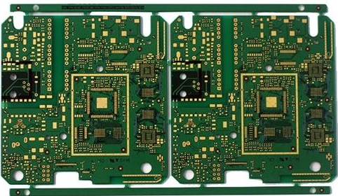
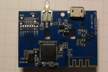
The quality and reliability of surface mount products mainly depend on the manufacturability and reliability of components, electronic process materials, process design and assembly processes. In order to successfully assemble PCBAproducts, on the one hand, the quality of electronic components and process materials needs to be strictly controlled, that is, incoming material inspection; on the other hand, the assembly process must be reviewed for the manufacturability (DFM) of the SMT process design. After and before each process in the implementation process, process quality inspection should also be carried out, that is, surface assembly process inspection, which includes quality inspection methods and strategies for each process of the entire assembly process such as printing, patching, and welding.
1) Inspection content of solder paste printing process
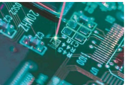
Solder paste printing is the initial link in the SMT process. It is the most complex and unstable process. It is affected by multiple factors and has dynamic changes. It is also the source of most defects. 60% -70% of defects appear. In the printing stage. If an inspection station is set up after printing to conduct real-time inspection of the solder paste printing quality and eliminate defects in the initial links of the production line, losses and costs can be minimized. Therefore, more and more SMT production lines are equipped with automatic optical inspection for the printing process, and even some printing machines have integrated solder paste printing system such as AOI. Common printing defects in the solder paste printing process include non-turning solder on the pad, excessive solder, solder paste scratching in the middle of the large pad, solder paste sharpening at the edge of the small pad, printing offset, bridging, and contamination. Wait. The reasons for these defects include poor solder paste fluidity, improper template thickness and hole wall processing, unreasonable printer parameter settings, insufficient precision, improper selection of blade material and hardness, and poor PCB processing.
SMT processing factory 6 2) Inspection content of component placement process The placement process is one of the key processes of the SMT production line. It is one of the key factors that determine the degree of automation, assembly accuracy and productivity of the assembly system. It has a decisive impact on the quality of electronic products. Therefore, real-time monitoring of the placement process is of great significance to improve the quality of the entire product. The inspection flow chart before the furnace (after placement) is shown in Figure 6-3. Among them, the most basic method is to configure the AOI after the high-speed placement machine and before the reflow soldering to inspect the quality of the placement. On the one hand, it can prevent the defective solder paste printing and placement from entering the reflow stage, thereby bringing more On the other hand, it provides support for the timely proofreading, maintenance and maintenance of the placement machine, so that it is always in good operating condition. The inspection content of the placement process mainly includes the placement accuracy of the components, the control of the placement of fine-pitch devices and BGA, various defects before reflow soldering, such as missing components, offset, solder paste collapse and offset, PCB The board surface is contaminated, the pins are not in contact with the solder paste, etc. Use character recognition software to read the value and polarity recognition of the components, and judge whether the pasting is wrong or reversed. 3) Inspection content of welding process Inspection after welding requires 100% inspection of the product. Usually need to check the following content: check whether the solder joint surface is smooth, whether there are holes, holes, etc.; check whether the solder joint shape is half moon shape, whether there is more tin or less tin phenomenon; check whether there are tombstones, bridges, component shifts, Missing components, tin beads and other defects; check whether all components have polarity defects; check whether there are short circuits, open circuits and other defects in soldering; check the color change of the PCB surface.