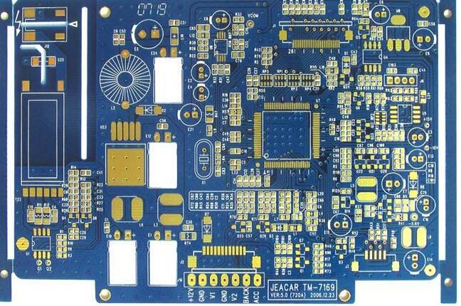
The structure of industrial PCB is much more complicated, and the occasion of use is much more complicated than ordinary PCB.
Industrial PCB requires professional designers, skilled workers, high-quality industrial equipment and excellent manufacturers.
These PCBs are manufactured for long-term use. Therefore, the materials it uses are more durable than those used in ordinary PCBs.
Industrial PCBs must be manufactured very carefully to have many specifications.
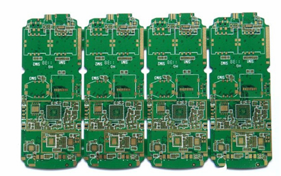
Not all PCB manufacturers can manufacture industrial PCBs because of the complex manufacturing process of industrial PCBs.
Therefore, it is very important to find a suitable manufacturer after PCB design.
The use of robotics and automation in industrial operations is increasing.
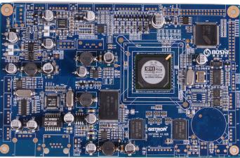
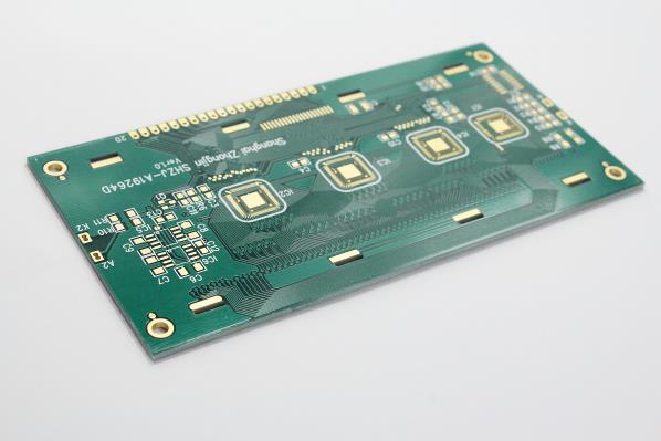
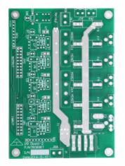
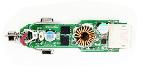
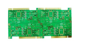
Industrial PCBs are widely used in power control systems, industrial smart meters, industrial lighting systems and other fields.
Industrial PCBs are designed for long-term use. These cannot be replaced as often as ordinary PCBs.
In other words, we must pay attention to quality, reliability and performance when manufacturing.

The main reason for this is that all companies want to reduce labor costs and try to improve accuracy and efficiency.
PCB is an important factor in robotics and automation. And this type of PCB must have industrial-grade reliability, precision and flexibility.
PCBs used in the industrial sector must be flexible, durable, and prepared for harsh conditions. Now we will discuss some key points about industrial PCBs.
What is an industrial PCB?
Simply put, the PCB used in the industrial field is called the industrial PCB.
High-profile PCBs are used in various industrial applications.
These are called industrial PCBs. Like other PCBs, industrial PCBs have multiple layers, and each conductive layer is separated by an insulating material.
The insulating material is usually made of glass fiber, plastic or ceramic.
The normal standard for PCB materials is PIC2221A.
This standard must be maintained for all types of PCBs.
If designers want to use power conversion devices, IPC9592 recommends additional parameters.
Many of the cutting-edge technologies we see today rely heavily on PCBs. Industrial PCBs have contributed to the automation of many industries.
Thanks to the industrial PCB, the robotic arms used in various product manufacturing units can work smoothly and accurately. Now we will learn more about industrial PCBs.
Industrial PCB composition:
Many types of materials are used to make industrial PCBs.
Here, layers of different materials are bonded together by means of adhesives under extreme heat and pressure. The side view of the PCB looks a lot like a layered cake.
Now let us analyze each layer of the PCB.
Our main goal is to analyze what material each layer is made of and what its function is.
Substrate:
The material used to make the PCB base layer is called the PCB base layer material. This type of primer is commonly referred to as a substrate.
It is usually made of glass fiber material. Almost all types of PCB use FR4 type glass fiber. Because it tends to be very tough in nature.
The reason for using this hard material on the PCB substrate is that the substrate strengthens the other layers of the PCB.
In the case of a flexible PCB, the substrate is flexible. The substrate is usually made of flexible plastic.
PCB thickness ranges from 0.6mm to 1.6mm. However, other materials can also be used to make PCBs.
However, other materials can also be used to make PCBs. As epoxy resins and phenolic resins, they are used in many PCBs.
One thing we need to remember is that the substrate needs to be hard enough so that the PCB can be used in industry.
This is why glass fiber is most useful in all these situations.
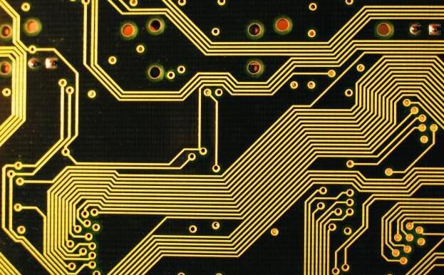
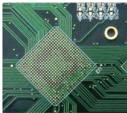
Copper layer:
After the base layer, the most important layer is the copper layer.
This copper layer plays an important role in keeping the PCB active.
Under extreme heat and pressure, the copper layer is laminated to the base layer with the aid of an adhesive.
In the case of double-layer and multilayer PCBs, there are copper layers on both sides of the layer.
Industrial PCBs usually do not use copper layers, because all these PCBs have many complex tasks to perform.
The thickness of the copper layer varies from PCB to PCB. Since industrial PCBs operate at higher power, their thickness is 2-3 ounces.
This means that in all these cases, the thickness of the copper layer is 35um.
This copper layer is the main conductive layer of the PCB, that is, all kinds of work are done here.
To print the required circuit pattern on the substrate, you can use two methods.
One is addition and the other is subtraction.
In the additive method, copper will be coated on the surface of the substrate according to our desired pattern, while the rest of the area will remain uncoated. Most consumer PCBs are printed in this way.
In the subtractive method, you first need to cover the entire substrate surface with copper, and then according to the design, remove unnecessary areas, that is, remove the coating material in those areas.
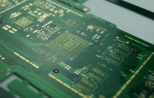
Welding mask:
The most important layer after the copper layer is the solder mask. The green color we see on the PCB is due to this solder mask.
This is the top layer of the copper layer. Protect the various traces, paths and components of the PCB from any external conductive materials.
It can also play a shielding role in the welding process, so that no short circuit occurs. Simply put, it can protect the PCB from any unwanted external connections.
Silk printing:
Use a silk screen layer on top of the solder mask. It helps to mark the names, values, locations, and pin configurations of various components on the PCB.
It is very important to mark all these important things with silk screen printing. This is because all this information helps to place the components in a shorter time and in a perfect way when assembling the PCB. In addition, if any PCB board is damaged, the brand's silk screen helps to replace specific components.
Layer-based industrial PCB types:
PCB manufacturing is usually much more difficult than designing a PCB. Over time, designers try to figure out how to design a single circuit by integrating multiple circuits on the same platform.
With the innovation of new technologies, PCB manufacturers are facing increasing challenges.