When designing PCBA to place special components, first consider the size of the PCB. When the size of PCB board is too large, the printing line is too long, the impedance increases, the dry resistance decreases, and the cost increases; If it is too small, the heat dissipation is poor, and adjacent lines are vulnerable to interference. After determining the PCB board size, determine the square position of the special parts. Finally, all components of the circuit are arranged according to the functional unit. The location of special components shall generally follow the following principles:
1) Shorten the connection between high-frequency components as much as possible, and reduce their distribution parameters and mutual electromagnetic interference as much as possible. The easily disturbed parts shall not be too close, and the input and output shall be as far away as possible.
2) Some components or wires may have high potential difference, so the distance between them should be increased to avoid accidental short circuit caused by discharge. High voltage components shall be kept out of reach as far as possible.
3) Components weighing more than 15g can be fixed with brackets and then welded. These heavy and hot components should not be placed on the PCB board, but on the bottom plate of the main box, and heat dissipation should be considered. Hot parts shall be far away from heating components.
4) For the layout of adjustable components such as potentiometer, adjustable inductance coil, variable capacitor and microswitch, the structural requirements of the whole wrench shall be considered. If the structure allows, some commonly used switches shall be placed in positions easily accessible by hands. The layout of components shall be balanced, dense and not heavier than the top.
For the success of a product, the first is to pay attention to the internal quality. But considering the overall beauty, both are relatively perfect wrenches, which can become successful products.

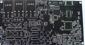
Special components of PCB board refer to the key components of the high-frequency part, the core components in the circuit, the components that are vulnerable to interference, the high-voltage components, the high calorific value components and some heterosexual components. The position of these special components needs to be carefully analyzed to make the belt layout meet the circuit function and production requirements. Improper placement may cause circuit compatibility problems and signal integrity problems, leading to PCB design failure.
It is believed that many people will face a problem when making high-frequency PCB: how to solve the power noise interference on high-frequency PCB board? Technicians said that it can destroy the occurrence conditions and effectively suppress power noise interference. The specific solutions are as follows:
1) Pay attention to the through holes on the plate. The through hole makes it necessary to etch the opening on the power layer to leave space for the through hole to pass through. If the power supply layer is too large, it will inevitably affect the signal circuit, forcing the signal bypass, increasing the circuit area and noise. At the same time, if some signal lines are concentrated near the opening and share this section of circuit, the common impedance will cause crosstalk.
2) Place the power noise filter. It can effectively suppress the noise inside the power supply and improve the anti-interference and safety of the system. In addition, it is a bidirectional RF filter, which can not only filter the noise interference introduced by the power line (to prevent interference from other devices), but also filter the noise generated by itself (to avoid interference with other devices), and suppress the serial mode common mode interference.
3) Power isolation transformer. Separate the power circuit or common mode grounding circuit of the signal cable, which can effectively isolate the common mode circuit current generated by high frequency.
4) Power regulator. Getting a cleaner power supply can greatly reduce power supply noise.
5) Wiring. The input and output lines of the power supply shall not be arranged at the edge of the dielectric plate, otherwise it is easy to generate radiation and interfere with other circuits or equipment.
6) Analog power supply and digital power supply shall be separated. High frequency equipment is usually very sensitive to digital noise, so they should be separated and connected together at the power inlet. If the signal crosses the analog and digital parts, the loop can be set at the signal intersection to reduce the loop area.
7) Avoid overlapping of independent power supplies between different layers. Stagger them as much as possible, otherwise the power supply noise is easily coupled through parasitic capacitors.
8) Isolate the sensitive element. Some components, such as phase-locked loop (PLL), are very sensitive to power supply noise. They should be as far away from the power supply as possible.
9) The connecting wire needs enough ground wire. Each signal shall have its own special signal loop, and the loop area of signal and loop shall be as small as possible, that is, the signal and loop shall be parallel.
10) Place the power cord. In order to reduce the signal circuit, the noise can be reduced by placing the power line close to the signal line.
11) In order to prevent the power supply noise interference on the PCB board and the accumulated noise caused by the external interference on the power supply, the bypass capacitor can be grounded on the interference path (excluding radiation), so as to bypass the noise to the ground and avoid interference with other equipment and devices.
The power supply noise is directly or indirectly generated by the power supply and interferes with the circuit. When restraining its influence on the circuit, we should follow a general principle, that is, on the one hand, we should try to prevent the influence of power supply noise on the circuit. On the other hand, we should also try to reduce the impact of external or PCB board on the power supply to avoid the deterioration of power supply noise.