1. Cause:
1) The melting time of the solder paste at both ends of the PCBA component is not synchronous or the surface tension is different. Generally, the end melted after the solder paste is pulled up.
2) Pad design: The pad extension length has an appropriate range, and if it is too short or too long, it is easy to erect a tablet.
3) If the solder paste is too thick, the components will float after melting.
4) Setting of temperature curve: the erection of a monument generally occurs at the moment when the solder joint begins to melt, and the heating rate near the melting point is very important.
5) One welding end of the component is oxidized or contaminated and cannot be wetted.
6) Pads are contaminated.

2. Solution:
1) Design
The pad shall be designed reasonably, and the extension size shall be reasonable. The wetting angle of the pad's outer edge formed by the extension length shall not be greater than 45 °.
2) Production site
A. Wipe the screen frequently to ensure that the solder paste molding pattern is complete.
b. The placement of the patch is accurate.
c. Use non eutectic solder paste and reduce the heating rate during reflow welding.
d. Reduce the thickness of solder paste.
3) Incoming materials
Strictly control the quality of incoming materials to ensure that the effective area of both ends of the components used are the same.
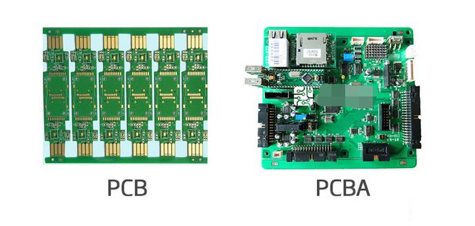
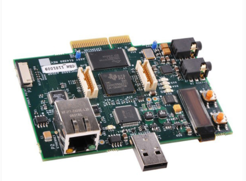
To understand which link has the highest cost, we need to break down the whole PCBA processing link. PCBA processing includes two parts: circuit board optical board and component welding (i.e. smt surface mounting+DIP plug-in post welding). At present, the prices of plates and components on the market are basically open and transparent, which can be compared and referred to. In addition to PCB and components, the cost is reflected in the assembly process. The main costs of this link are as follows:
1) Auxiliary materials: solder paste, tin bar, flux, UV glue, furnace fixture;
Solder paste and tin bar are the most important auxiliary materials in the whole processing process. For the same welding area, the price of imported solder paste is much higher, but the difference in welding quality is very obvious.
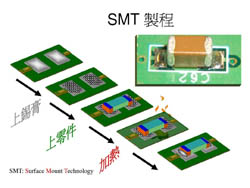
2) SMT chip processing:
The price of chip processing will vary according to the number of points and packaging. It is the consensus in the industry that the quantity is large and the price is excellent; The larger the package size of components, the easier it is to mount them, and the corresponding defective rate will be reduced, so there is more room for price communication.
3) Welding time cost after DIP plug-in:
Because it involves the forming of special-shaped parts and materials, this link requires a lot of manual participation, which is the most difficult to control the cost. At present, the labor cost remains high, and the cost of this link is generally high.
4) PCBA Assembly test: test fixture, test equipment, test man hours.
The price of test fixture varies according to the test difficulty. Sometimes, it also needs optical fiber, ICT and other test equipment. The corresponding labor and equipment losses should be taken into account, but the test price will not be very high; Some PCBA companies even test for free.