With the wide application of PCBA electronic products, the reliability of electronic products has become a prominent problem. Most applications require electronic products to operate stably, reliably and safely. In aviation, aerospace, military, communications, finance, monitoring and other fields, the failure and failure of electronic systems may cause huge losses.

The reliability of electronic products and systems is particularly complex because electronic products are composed of electronic components, printed circuit boards, solders, accessories and software with complex types and different materials. From the perspective of electronic product manufacturing, electronic manufacturing can be divided into four levels, namely, level 0 (semiconductor manufacturing), level 1 (PCB design and manufacturing, IC packaging, manufacturing of passive components, manufacturing of process materials and other electromechanical components), level 2 (board level assembly of electronic products), and level 3 (overall assembly of electronic products). Corresponding to four levels of classification, the reliability of electronic products can also be divided into four aspects. The system level reliability of electronic products corresponds to the assembly of the whole machine, the board level process reliability corresponds to the board level process reliability, that is, the reliability of surface assembly process, the reliability of components corresponds to the packaging, components and process materials, and the reliability of semiconductor manufacturing corresponds to the reliability of semiconductor process.
The reliability design of electronic assembly process includes three aspects: simulation design, failure analysis and reliability test. The business development and staffing of the process reliability department of the industry leading large electronic companies are basically based on this framework. These three aspects can meet the requirements of assembly process reliability from qualitative analysis to quantitative design. But for most small and medium-sized electronic companies, it is difficult to establish such a huge system and organize a complete reliability department and design process. For them, a more effective method is to establish their own electronic assembly process reliability specifications or guidelines to guide how to take measures to ensure reliability requirements in PCB design stage, PCBA assembly process, process failure analysis and process reliability testing, and when new processes appear.
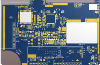
Hole (Via) is an important part of multilayer PCB, and the drilling cost usually accounts for 30%~40% of PCB production cost. Therefore, via design has become an important part of PCB design. In short, each hole on a PCB can be called a via. From the perspective of function, vias can be divided into two categories: one is used as an electrical connection between layers; Second, it is used for fixing or positioning devices. In terms of process, these vias are generally divided into three categories, namely blind hole, buried hole and through hole.
The blind hole is located on the top and bottom surfaces of the printed circuit board, and has a certain depth. It is used to connect the surface line and the lower inner line. The depth of the hole usually does not exceed a certain ratio (aperture). Embedded hole refers to the connection hole located in the inner layer of the printed circuit boards, which will not extend to the surface of the printed circuit board. The embedded hole is located in the inner layer of the circuit board and is completed by the through hole forming process before lamination,
During hole formation, several inner layers may be overlapped. The third kind of hole is called through hole, which passes through the whole circuit board and can be used for internal interconnection or component installation positioning hole. Because the through-hole is easier to realize in technology and lower in cost, most printed circuit boards use it instead of the other two kinds of through-hole. From the design point of view, a through-hole is mainly composed of two parts: one is the drilling hole in, and the other is the pad area around the drilling hole. The size of these two parts determines the size of the vias.
Obviously, when designing high-speed PCB and high-density PCB, circuit board designers always hope that the smaller the hole, the better, so that more wiring space can be left on the PCB; In addition, the smaller the vias are, the smaller their parasitic capacitance is, which is more suitable for high-speed circuits. However, the reduction of hole size also brings about an increase in cost, and the size of vias cannot be infinitely reduced, which is limited by drilling and electroplating technology. The smaller the hole, the longer it takes to drill and the easier it is to deviate from the center. As far as the current PCB manufacturing technology is concerned, when the ratio of PCB substrate thickness to aperture (i.e. thickness diameter ratio) exceeds 10, it is impossible to ensure uniform copper plating on the hole wall, while the copper layer thickness is uneven, especially in the middle of the coating, will seriously affect the fatigue life of the PCB board hole.