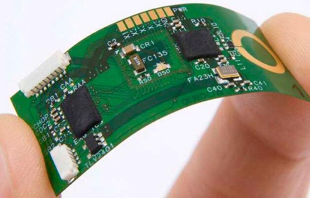
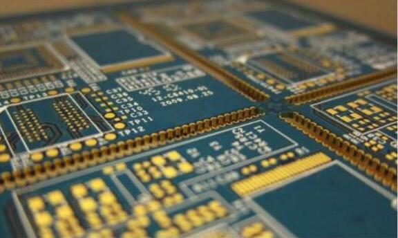
In the process of SMT PCB assembly, testing, transportation and use, the corresponding mechanical stress will inevitably be generated. When the mechanical stress exceeds the stress limit of some components and wiring, it will lead to cracks in the components, and even lead to cracking and failure of the components, seriously affecting the reliability of the product. Multi-layer ceramic capacitor (MLCC), a common stress-sensitive element, is more sensitive to stress, especially the large-size MLCC.
Common occasions for generating mechanical stress include:
1) The mechanical stress generated by the tip during the placement process
2) After welding, if there is large warpage deformation on the PCB board, the mechanical stress generated when the plate deformation recovers during the assembly of the whole machine
3) Mechanical stress produced by pcb in the process of segmentation
4) Mechanical stress generated during ICT test
5) Mechanical stress generated during screw tightening
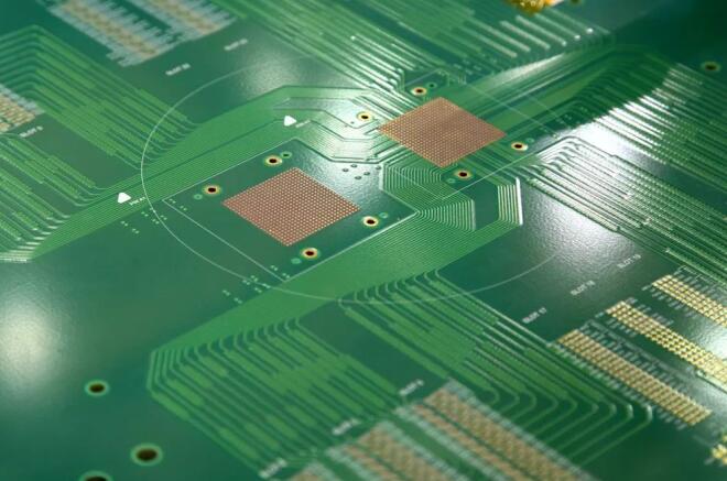
From the perspective of reliability design, the reliability problems caused by mechanical stress can be improved from the aspect of layout. The basic principle is that the stress-sensitive components, such as MLCC, should be considered in the stress-proof area and avoid the high-stress area. For example, when dividing boards, the stress generated in devices with different layout directions is different. The stress generated in devices parallel to the auxiliary edge will be smaller than those perpendicular to the auxiliary edge. Therefore, there are also requirements for layout direction in addition to not arranging devices in the forbidden area. Similarly, different deformation directions of PCB have different effects on physical examination. When the PCB produces the deformation direction as shown in the figure, the long side of the layout component is consistent with the deformation direction, the internal stress of the component is large, and the stress in the opposite direction is small.

According to the production and use of electronic products, reliability screening can be divided into finished product screening, process screening of device production line and screening before use by the complete machine PCB factory. The following is a brief introduction to some commonly used screening methods.
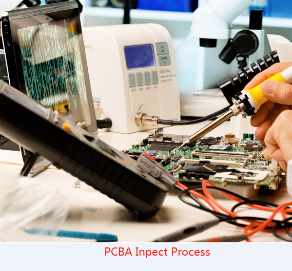
1) Visual and microscopic screening
Visual inspection or microscopic inspection (microscopic inspection) is an important screening method in the manufacturing of electronic products. It can be used to find and remove dirt, defects, damage and poor connection. The microscopic inspection standard should be reasonably formulated according to the main failure mode and mechanism, and combined with the specific failure process. Years of experience has recognized that this method is one of the most simple and efficient methods. It is very effective for checking various defects on the chip surface (such as metallized layer defects, chip cracks, oxide layer quality, mask quality and diffusion defects, etc.), as well as observing inner lead stitching, chip welding and packaging defects. In foreign countries, there are automatic microscopy systems that use scanning electron microscope and computer.
2) X-ray screening
X-ray is a kind of non-destructive screening, which is used to check whether there are residues in the shell, potential defects in bonding and packaging processes and cracks on the chip after the device is sealed.
3) Infrared filtering
The characteristics of heat distribution (hot spots and hot areas) are revealed by infrared detection or photography. When the design is unreasonable, there are defects in the process and there are some failure mechanisms in the production
process, a hot spot or hot zone will be generated in a part of the product. In this way, unreliable components can be pre-screened. The advantage of infrared screening is that it does not damage components in the inspection process, especially in the inspection of large-scale integrated circuits.
4) Power aging
Power aging is a very effective screening method and one of the necessary screening methods for high integrated circuits. Power aging can eliminate the potential defects of early failure devices as soon as possible by applying excessive electrical stress to the products. It can effectively eliminate the process defects, too thin metallized film, scratches and surface contamination produced in the device production process. Power aging usually refers to placing integrated circuit products at high temperature and applying maximum voltage to obtain enough screening stress to eliminate early failure products at high temperature and applying maximum voltage to obtain enough pulse power aging. The former is mostly used in small-scale digital circuits, while the latter is used in medium and large-scale integrated circuits, so that the components in the circuit can withstand the maximum power consumption and stress under working conditions when aging. Although the ultra-power aging can shorten the aging time, it can also make the instantaneous load of the device exceed the maximum rated value, and cause the qualified device to suffer damage, even instant deterioration or breakdown. Some products may still work temporarily, but their service life is shortened. Therefore, for over-power aging, it is not that more overload is more effective, but the best overload should be selected. At present, the more consistent method is to apply the maximum rated power to the device and appropriately extend the aging time, which is a more reasonable electric power aging screening method.
5) Temperature cycling and thermal shock screening
Temperature cycling can accelerate the failure caused by thermal mismatch between materials. Potential defects such as chip assembly, bonding, packaging and metallized film on the oxide layer can be screened through temperature cycling. Typical conditions for temperature cycle screening are - 55~+155 ℃ or - 65~+200 ℃ for 3 or 5 cycles. Each cycle shall be kept for 30min at the highest or lowest temperature, and the transfer time shall be 15min. The AC and DC parameters shall be tested after the test. Thermal shock screening is an effective method to determine the strength of integrated circuits with sharp temperature changes. For example, two water tanks of 100 ℃ and 0 ℃ are set, which are taken out after soaking in the high temperature tank for 15s, and then moved into the low temperature tank for at least 5s within 3s, and then moved into the high temperature tank within 3s. Repeat for 5 times. For some products, if the thermal expansion and contraction properties of the internal parts materials do not match, or the parts have cracks, or the defects caused by the poor SMT process, the early failure parts can be made to fail in advance under the temperature impact of high and low temperature alternating environment. This method has good screening effect.
6) High temperature storage screening
High temperature can accelerate the chemical reaction inside the product. If there is water vapor or various harmful gases in the shell of integrated circuit package, or the chip surface is not clean, or there are different metal components at the bonding point, chemical reactions will occur, and high temperature storage can accelerate these reactions. Because this screening method is easy to operate, can be carried out in batches, has good screening effect and low investment, so it is widely used.
7) High temperature work screening
High-temperature working screening generally includes three screening methods: high-temperature DC static, high-temperature AC dynamic and high-temperature reverse bias, which is very effective for eliminating the failure caused by the potential defects on the device surface, body and metallization system. High temperature reverse bias is a test of adding reverse bias working voltage at high temperature. It is carried out under the joint action of hot spots, which is very close to the actual working state. Therefore, the effect of PCB board screening is better than that of simple high temperature storage.