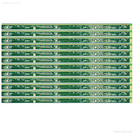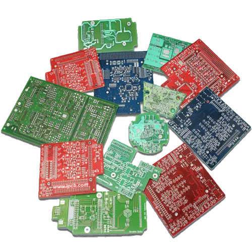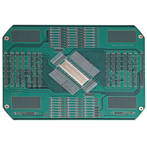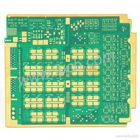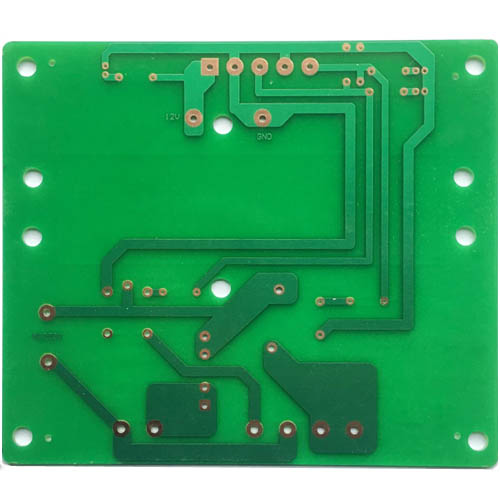


Model: PWB Manufacturing
Material: FR-4, High TG FR-4
Layer: 2 Layer - 70 Layer
Color: Green/Black/Blue/White
Finished Thickness: 0.4mm - 6.0mm
Copper Thickness: 1/H/H/1 OZ
Surface Treatment: Gold/HASL/OSP
Min Trace: 3mil, 0.075mm
Min Space: 3mil, 0.075mm
Application: Electrical apparatus, industrial PCB, automotive PCB, airplane PCB
iPCB company is a famous PWB manufacturer, we provide PWB manufacturing, PWB design, and PWB assembly. Our quality service helps your products to occupy the market.
PCB vs PWB
PCB is a printed circuit board, and PWB is a printed wiring board. So PCB and PWB mean that they are all carriers of interconnected circuits that use conductors to form devices on insulating substrates. It's just that different countries have different customary names. The Chinese like to call it PCB, while the British used to call it PWB in the early days.
The 50-year history of PWB manufacturing technology development can be divided into six periods
1. PWB Born 1936~Manufacturing Method Addition
The pattern of conductive material added to the insulation plate surface to form the conductor is called the additive process The patented printed board used in this type of production was used in radio receivers at the end of 1936.
2. PWB Manufacturing Trial Period 1950~Manufacturing Method Subtraction Method
The manufacturing method is to use copper-clad paper-based phenolic resin laminate PP base material to dissolve the unwanted copper foil with chemicals and make the copper foil into an electrical circuit called the reduction process. In some label manufacturing factories, this process is used to try out PWB with manual operation as the main corrosive liquid. If iron trichloride splashes on clothes, it will turn yellow.
The typical product that used PWB at that time was the one-sided PWB of the portable transistor radio made by Sony and the PP base material.
3. PWB Manufacturing Trial Period 1960~New Material GE Material Appeared
PWB application copper-clad glass cloth epoxy resin laminate GE base material Due to problems such as heating warping and deforming copper foil peeling of PWB's domestic GE base plate at the beginning, material manufacturers have gradually improved. Since 1965, several Japanese material manufacturers have started mass production of GE base plate for industrial electronic equipment PP base plate for civil electronic equipment has become common sense.
4. PWB Manufacturing Drop-in Period 1970~MLB Comes on Stage New Installation Method
During this period, PWB developed from 4 layers to more layers, and the width and spacing of thin-wired, thin-hole, and thin-plate lines with high density were expanded from 0.5mm to 0.350.20.1mm. Wiring density per unit area of PWB was greatly increased. The installation mode of components on PWB started to change revolutionarily. The original insert installation technology TMT was changed to surface installation technology SMT lead insert installation method, which has been used on PWB for more than 20 years and has also been developed by manual operation. Automatic component inserter for automatic assembly line SMT uses an automatic assembly line for PWB mounting components on both sides.
5. MLB Leap Period 1980~Ultra-high density installations
The output value of Japanese PWB increased approximately threefold in the 10 years from 1982 to 1991. The output value of Japanese PWB in 1982 was 361.5 billion yen in 1991 was 109.4 billion yen in 1991. In 1986, 146.8 billion yen overtook the output value of a single panel, and in 1989, 278.4 billion yen approached the output value of a double panel. PCB densification significantly increased after 1980. The production of 62-layer glass-ceramic-based MLB densification has driven competition for mobile phone and computer development.
6. Run-up Period Towards 21st Century 1990~MLB Stacked
After 1991, the impact of Japan's bubble economy on electronic equipment and PBB declined to 1994 before resuming substantial growth in MLB and flexible panels, while single- and double-panel production began to decline. Since 1998, MLB with the stacking method has entered a trial period, and its output has increased rapidly. IC component packaging has entered into BGA and CSP of polygon array end-connector to miniaturize and ultra-dense installation.
Future Prospects
Over the past 50 years, the development of PWB manufacturing technology has greatly changed since the invention of the semiconductor transistor in 1947. Semiconductors have developed higher integrated IC such as MCM, BGA, CSP from IC, ISIV, LSI to high integration. The technological trend in the early 21st century is to dominate the innovative technology in the 21st century for the sake of high-density miniaturization and lightweight devices. The research and development of electronic components will be driven by nanotechnology.

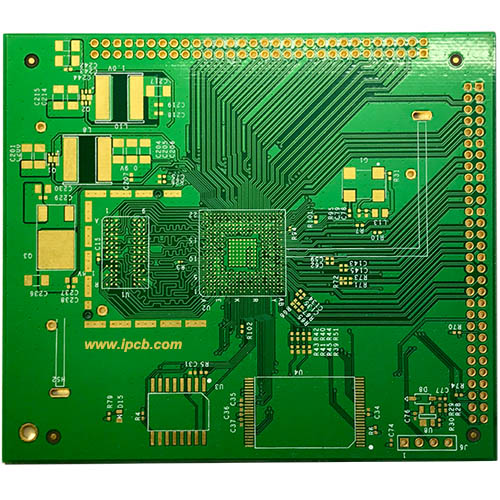
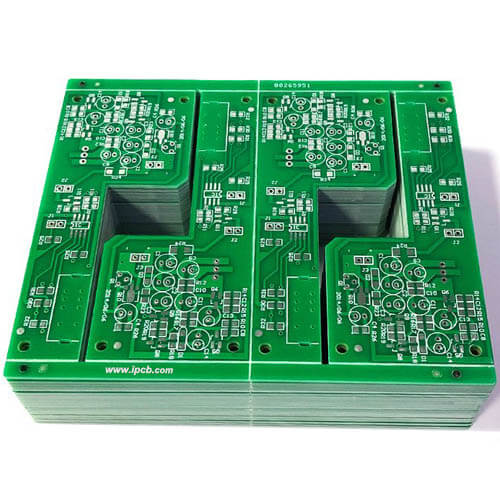
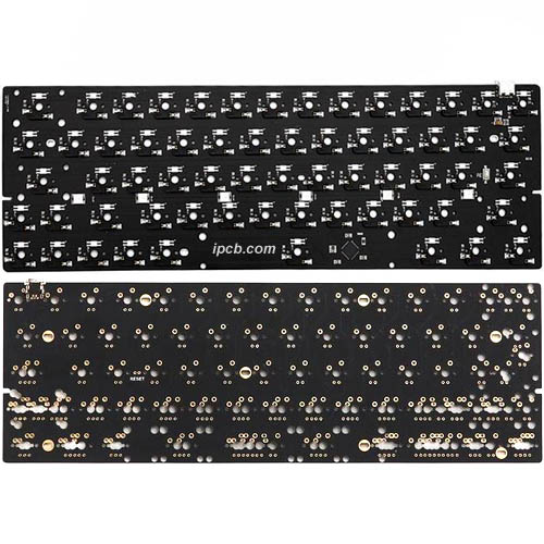
Model: PWB Manufacturing
Material: FR-4, High TG FR-4
Layer: 2 Layer - 70 Layer
Color: Green/Black/Blue/White
Finished Thickness: 0.4mm - 6.0mm
Copper Thickness: 1/H/H/1 OZ
Surface Treatment: Gold/HASL/OSP
Min Trace: 3mil, 0.075mm
Min Space: 3mil, 0.075mm
Application: Electrical apparatus, industrial PCB, automotive PCB, airplane PCB
For PCB technical problems, iPCB knowledgeable support team is here to help you with every step. You can also request PCB quotation here. Please contact E-mail sales@ipcb.com
We will respond very quickly.