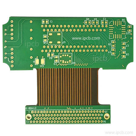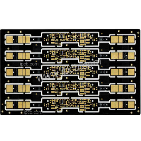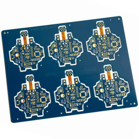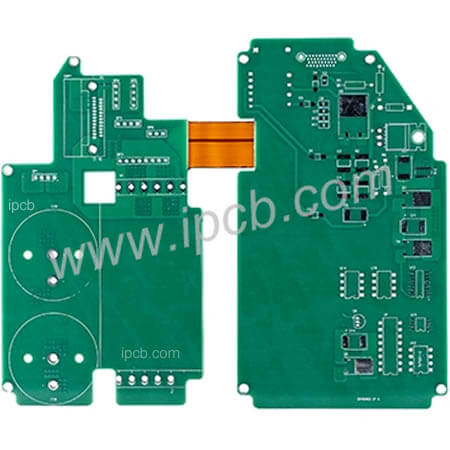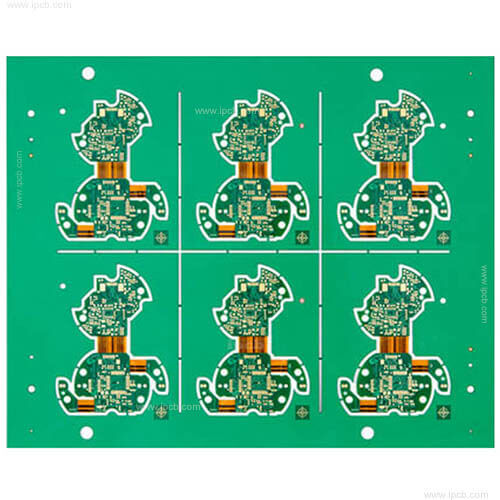
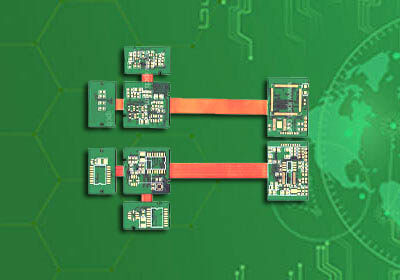

Model : 6Layers Rigid-Flex PCB
Material : FR-4+PI
Layer : 2+2+2
Color : Green/White
Finished Thickness : 1.0mm
Copper Thickness : 1OZ
Surface Treatment : ENIG 2U"
Minimum line width / distance : 0.15/0.15mm
Application : Medical treatment Rigid-Flex PCB
The protective material of the Rigid-Flex PCB outer layer pattern, that is, the solder mask, generally has three types to choose from. The first type is the traditional cover film (Coverlay), which is a direct layer of polyimide material and adhesive. It is laminated with the circuit board that needs to be protected after etching. This kind of cover film requires pre-formed before pressing, exposing the part to be welded, so it cannot meet the requirements of finer assembly. The second type is photosensitive development type cover dry film, After pressing with the laminator, the welding part is leaked through the photosensitive development method, which solves the problem of assembly fineness. The third type is liquid screen printing type covering materials, and thermosetting polyimide materials are commonly used, such as solar PSR-4000 and special solder resist ink for photosensitive development type flexible circuit boards, these materials can better meet the requirements of fine-pitch, high-density assembly of flexible boards.
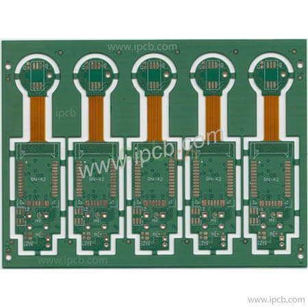
Rigid-Flex PCB production process and control of key parts
Rigid-Flex PCB is developed on the basis of flexible PCB board and high-density multilayer rigid PCB boards. It has many similarities with rigid PCB boards in terms of process manufacturing. However, due to Rigid-Flex PCB materials and their The particularity of structure and application determines that it is different from ordinary rigid PCB boards and flexible PCB boards from design requirements to manufacturing processes. Almost every production link must be tested and adjusted to optimize the entire process. Process and parameters.

Rigid-Flex PCB production process
Pattern transfer of Rigid-Flex PCB inner layer monolithic
Graphic transfer occupies a very important position in high-density, thin-line PCBs, especially for flexible circuits. Because the flexible monolith is thin and soft, it brings great difficulties to operations such as surface treatment, and the clean state and roughness of the surface of the copper foil directly affect the adhesion of the resist dry film and the production of fine lines. Since mechanical wiping requires high equipment, and unsuitable pressure may cause substrate deformation, curling, size expansion, etc., the operation is not easy to control, so we can choose to use the electrolytic cleaning method. This method can not only ensure the surface cleanliness, but also use the micro-etching method to ensure the roughness of the copper surface, which is conducive to the production of line patterns with a line width/spacing of 0.1mm~0.15mm. In acid etching, in addition to controlling the etching rate to ensure the line width and spacing required by the design, it is also necessary to prevent the single chip from curling and wrinkling. It is best to add an auxiliary guide plate and close the ventilation system on the equipment.
Multi-layer positioning of flexible materials
The dimensional stability of flexible substrates is poor. This is because polyimide materials have strong moisture absorption. After wet treatment or in different temperature and humidity environments, they shrink and deform seriously, resulting in layers of multi-layer PCB. Difficulty in counterpointing. In order to overcome this difficulty, the following measures can be adopted: in the design, the design of the alignment motifs and target punching spots should be considered, so as to ensure the accuracy when punching the alignment holes or rivet holes, and not cause them when stacking plates. The misalignment of the graphics between layers leads to scrapping.
Positioning holes after OPE punching can eliminate errors caused by material expansion and contraction during wet processing.
After PCB lamination, use X-ray to drill holes to determine the offset to make the drilling more precise. According to the material characteristics and environmental characteristics of polyimide, the outer film is drawn with reference to the drilling offset to improve the overlap between the outer film and the drilling board. In this way, we can meet the requirement of 0.1mm~0.15mm ring width for interlayer registration, and ensure the accuracy of outer layer graphics transfer.
Rigid-Flex PCB lamination
Even if the positioning holes are punched with OPE, the single-chip processing before lamination has a great influence on the alignment between layers. First of all, because the polyimide material is not resistant to strong alkalis, it will swell in the strong alkali solution. Therefore, in the process of blackening and browning, the strong alkaline process such as degreasing, blacking and browning should be appropriately reduced. Temperature, reduce time. Since the base material without adhesive layer is used, there is no need to consider the change of the adhesive layer in the lye, this method is still feasible. Secondly, the single-chip baking after oxidation treatment should be avoided to be placed vertically, and horizontal baking should be adopted to reduce bending deformation and keep it as flat as possible. After baking, shorten the moulding time as much as possible to prevent the single piece from absorbing moisture again.
Because the flexible single sheet is easy to deform, the flatness before lamination is poor, and the resin fluidity of the adhesive sheet used is much lower than that of the prepreg used for rigid PCB board lamination. Therefore, in order to make the adhesive sheet and the single sheet good combination Embedded in the fine line spacing, we choose to use materials with better covering shape as the laminated gasket material, such as polypropylene film, polytetrafluoroethylene (PTFE), silicone rubber sheet, etc., which can improve the lamination of flexible boards. quality. After the test, it is believed that the ideal gasket material is a silicone rubber material, which can ensure its shapeability and relatively reduce the shrinkage and deformation of the pressed part.
For the PCB hard board part, the following three aspects should be paid attention to in the pressing process:
A. Whether it is PCB substrate lamination or pure prepreg lamination, the warp and weft directions of the glass cloth should be consistent, and the thermal stress should be eliminated during the lamination process to reduce warpage.
B. The PCB rigid board should have a certain thickness, because the flexible part is very thin and there is no glass cloth. After being affected by the environment and thermal shock, its change is different from the rigid part. If the rigid part does not have a certain thickness or Hardness, this difference will be very obvious, and serious warpage will occur during use, which will affect welding and use. If the rigid part has a certain thickness or hardness, this difference may appear insignificant. The flatness will not change with the change of the flexible part, which can ensure welding and use. If the rigid part is too thick, it will appear heavy and uneconomical. The experiment proves that the thickness of 0.8~1.0mm is more appropriate.
C. For the processing of flexible windows, there are usually first milling and post-milling methods to process, but it needs to be processed flexibly according to the structure and thickness of the Rigid-Flex PCB itself. If the flexible window is milled first To ensure the accuracy of milling, neither the welding nor the deflection should be affected too much. The milling data can be produced by the engineering, and the flexible window can be milled in advance. If you do not mill the flexible window first, and then use laser cutting to remove the waste material of the flexible window after completing all the previous processes and finally forming, you should pay attention to the depth of the FR4 that the laser can cut.
The pressing parameters can be comprehensively optimized with reference to the pressing parameters of the flexible substrate and rigid PCB board.
Rigid-Flex PCB drilling
The structure of Rigid-Flex PCB is complex, so it is very important to determine the best process parameters for drilling holes to obtain a good hole wall. In order to prevent the nail head phenomenon of the inner copper ring and the flexible base material, a sharp drill bit must be selected first. If the number of printed boards to be processed is large or the number of holes in the processed board is large, the drill bit must be replaced in time after a certain number of holes have been drilled. The speed and feed of the drill are the most important process parameters. When the feed is too slow, the temperature rises sharply and a lot of drilling dirt will be produced. If the feed is too fast, it is easy to break the drill bit, the adhesive sheet and the tearing of the media layer and the nail head phenomenon.
Secondly, the drilling machine should be selected and the drilling parameters should be optimized according to the plate thickness and the minimum drilling diameter. At present, there are drilling machines that can reach 200,000 revolutions per minute in the industry. For small holes, the higher the speed, the better the quality of the drilling. At the same time, the choice of cover and backing board is also very important. Good cover and backing board not only protect the board surface, but also play a good role in heat dissipation. It should be noted that the backing board is best to use aluminum foil board or epoxy glue board., Do not use paper backing plates, because paper backing plates are soft and are prone to serious drilling burrs. When deburring before boring, it is easy to tear or scratch the holes, which will bring trouble to the subsequent process and affect the Rigid-Flex PCB the quality of.
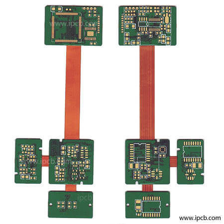
Model : 6Layers Rigid-Flex PCB
Material : FR-4+PI
Layer : 2+2+2
Color : Green/White
Finished Thickness : 1.0mm
Copper Thickness : 1OZ
Surface Treatment : ENIG 2U"
Minimum line width / distance : 0.15/0.15mm
Application : Medical treatment Rigid-Flex PCB
For PCB technical problems, iPCB knowledgeable support team is here to help you with every step. You can also request PCB quotation here. Please contact E-mail sales@ipcb.com
We will respond very quickly.