выбрать набор из шести навыков плата цепи design
The best плата цепи метод проектирования: при выборе необходимо учитывать шесть вещей плата цепи components based on component packaging. Все примеры в данной работе разработаны с использованием Multisim, but the same concepts still apply even with different EDA tools.
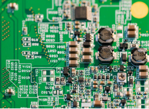
1. Consider the choice of component packaging
In the entire schematic drawing stage, Вы должны рассмотреть вопрос о принятии решений по упаковке и заземлению модулей на этапе компоновки. Some suggestions to consider when selecting components based on component packaging are given below.
. помнить, the package includes the electrical pad connections and mechanical dimensions (X, Y, and Z) of the component, То есть, the shape of the component body and the pins that connect to the плата цепи. Выбор компонента, you need to consider any installation or packaging restrictions that may exist on the top and bottom layers of the final плата цепи. Some components (such as polar capacitors) may have high headroom restrictions, which need to be considered in the component selection process. В начале проектирования, you can first draw a basic плата цепи форма рамок, and then place some large or position-critical components (such as connectors) that you plan to use. такой, the virtual perspective view of the плата цепи (without wiring) can be seen intuitively and quickly, и относительное положение устройства и высота его узла плата цепи and components can be given relatively accurate. This will help ensure that the components can be properly placed in the outer packaging (plastic products, chassis, каркас, etc.) after the плата цепи is assembled. Выберите из меню Сервис трехмерный предварительный просмотр плата цепи.

. The land pattern shows the actual land or via shape of the soldered device on the плата цепи. Эти медные узоры сверху плата цепи also contain some basic shape information. размеры рисунка паяного диска должны быть правильными для обеспечения правильной сварки и правильной механической и горячей целостности узлов соединения. проектировать плата цепи layout, Тебе нужно подумать. плата цепи will be manufactured, или если вручную сварить, как будет приваривать диск. Reflow soldering (the flux is melted in a controlled high temperature furnace) can handle a wide range of surface mount devices (SMD). обратная сторона сварной машины плата цепи to fix through-hole devices, Но он также может обрабатывать некоторые компоненты, вставленные на поверхности компьютера плата цепи. Generally, при использовании этой технологии, the bottom surface mount devices must be arranged in a specific direction, чтобы приспособиться к таким методам сварки, the pads may need to be modified.
. Выбор компонентов может быть изменен в течение всего процесса проектирования. Determining which devices should use plated through holes (PTH) and which should use surface mount technology (SMT) early in the design process will help the overall planning of the плата цепи. Factors that need to be considered include device cost, доступность, device area density, расход электроэнергии, and so on. с точки зрения обрабатывающей промышленности, surface-mount devices are generally cheaper than through-hole devices and generally have higher availability. Проект для малых и средних прототипов, it is best to choose larger surface mount devices or through-hole devices, не только ручная сварка, but also facilitate better connection of pads and signals during error checking and debugging.
. если в базе данных нет готовых пакетов, it is usually to create a customized package in the tool.
2. Use a good grounding method
Ensure that the design has sufficient bypass capacitors and ground planes. при использовании ис, make sure to use a suitable decoupling capacitor near the power terminal to the ground (preferably a ground plane). Соответствующая емкость конденсатора зависит от конкретного применения, capacitor technology and operating frequency. когда блокировочный конденсатор устанавливается между питанием и заземленным штырем, а также рядом с правильным выводом IC, можно оптимизировать электромагнитную совместимость и магнитную восприимчивость цепей.
3. Allocate virtual component packages
Print a bill of materials (BOM) for checking virtual components. Virtual components have no associated packaging and will not be transferred to the layout stage. создать таблицу Бом, а затем просмотреть все виртуальные детали. The only items should be power and ground signals, Потому что они считаются виртуальными компонентами, which are only processed in the schematic environment and will not be transmitted to the layout design. за исключением случаев, the components displayed in the virtual part should be replaced with encapsulated components.
4. Make sure you have complete bill of materials data
Check whether there is sufficient data in the bill of materials report. после создания отчёта, it is necessary to carefully check and complete the incomplete device, сведения о поставщике или изготовителе всех компонентов.
5. Sort according to component label
To facilitate the sorting and viewing of the bill of materials, make sure that the component numbers are consecutively numbered.
6. Check for redundant gate circuits
Generally speaking, все входы избыточных дверей должны иметь сигнальное соединение, чтобы избежать подвески входной зажим. Убедитесь, что проверка всех избыточных или недостающих дверей, and all unwired input terminals are fully connected. В некоторых случаях, if the input terminal is suspended, система не может работать нормально. Take the dual op amp that is often used in the design. если в модуле ис используется только один операционный усилитель, it is recommended to either use the other op amp, или включить в поле ввода неактивный операционный усилитель, and deploy an appropriate unity gain (or other gain) ) Feedback network to ensure that the entire component can work normally.
В некоторых случаях, ICs with floating pins may not work properly within the specification range. как правило, вход или выход близки или находятся на рельсах питания элемента только в том случае, если прибор IC или другая сетка в том же устройстве не работают в режиме насыщения, this IC can meet the index requirements when it works. Simulation usually cannot capture this situation, Поскольку аналоговые модели обычно не соединяют многие части интегральной схемы, имитируя эффект плавающего соединения