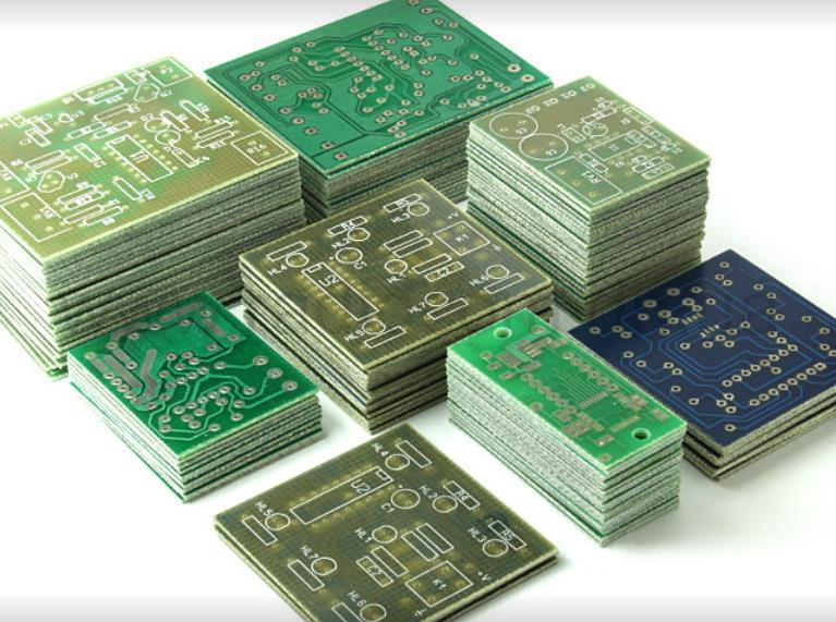
по мере того, как текущее проектирование портативной продукции идет в направлении миниатюризации и высокой плотности, PCB design is becoming more and more difficult, and higher requirements are put forward for the производство PCB процесс. In most of the current portable products, пакет BGA с высоким уровнем звука менее 0.65mm uses the design process of blind and утопленное отверстие. Так что же слепой и похороненный?
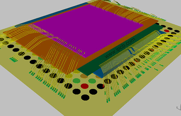
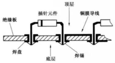
Blind vias (Blind vias / Laser Vias): Blind vias are vias that connect the inner traces of the PCB to the traces on the surface of the PCB. это отверстие не может пробить всю схему.
Buried vias: Buried vias are the type of vias that only connect the traces between the inner layers, Поэтому они не видны с поверхности PCB.
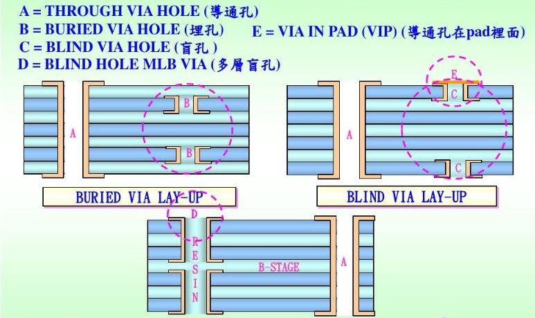
An 8-layer board:
A: Through hole (L1-L8)
B: Buried hole (L2-L7)
C: Blind hole (L7ï¼L8)
D: Blind hole (L1-L3)
2 Setting of blind and buried vias
Set Via type:
Click Setup-Pad Stacks in the menu, затем в "типе стека" выберите пункт пропускать, the settings dialog box as shown on the right will appear.
Нажмите кнопку Добавить отверстие в нижнем левом углу, чтобы указать тип прохода, including its drilling size, изометрический параметр.
If it is a through hole type, в нижнем левом углу выберите "пропустить", if it is a blind buried via type, select the Partial option
When selecting a Partial type via, Необходимо указать начальный и конечный уровни. For example, the blind and buried vias of the V12 and V27 types are set as shown in the figure below

3 PCB circuit board manufacturing process: blind and buried vias
When it comes to blind/buried vias, we start with traditional multilayer boards. Стандартная структура многослойная плита contains inner and outer circuits. процесс металлизации в скважинах и отверстиях используется для выполнения функции внутреннего соединения каждой цепи. Однако, because of the increase in circuit density, упаковка деталей непрерывно обновляется.
In order to allow the limited PCB area to place more high-performance parts, Помимо более тонкой ширины цепи, Эта апертура также уменьшена с 1 мм до 0 мм в отверстии DIP.6 mm in the SMD, и дальше до 0.4 мм или ниже. But it still occupies the surface area, Так что там были закопанные дыры и слепые дыры, which are defined as follows:
A. Buried Via
The through holes between the inner layers cannot be seen after pressing, so there is no need to occupy the area of the outer layer
B. Blind Via
Applied to the connection between the surface layer and one or more inner layers.
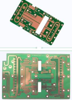
1. Buried hole design and production
The production process of buried vias is more complicated than that of traditional multilayer boards, и дороже стоит. Buried vias and general through holes and PAD size are generally specified.
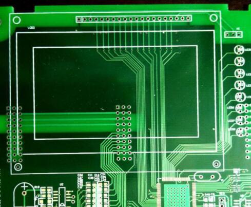
2. Blind hole design and production
The board with extremely high density, двухсторонний планшет, will have the outer layer up and down, А я/O vias will interfere with each other, especially when there is a VIP (Via-in-pad) design, it is even more troublesome. слепая дыра может решить эту проблему.