In general, если задержка межсоединений сигналов превышает пороговое время опрокидывания краевого сигнала на 20%, сигнальная линия на платы будет показывать эффект линии передачи, То есть, the connection is no longer a simple wire that displays lumped parameters. проявление, but showing the effect of distributed parameters, такой дизайн является высокоскоростным. In the design of high-speed digital systems, конструктор должен решить проблему перекоса и Искажения сигнала из - за паразитных параметров, timing and signal integrity issues. сейчас, this is also a bottleneck problem that проектирование высокоскоростных схемersmust solve.

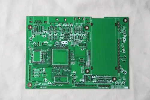
PCB proofing is driven by traditional physical rules
We can find that in traditional проектирование высокоскоростных схем, Настройки электрических и физических правил разделены. This brings the following shortcomings:
In the early stages of design, engineers had to spend a lot of energy on detailed front-end and back-end (that is, logical establishment-physical realization) analysis to plan a physical wiring strategy that meets electrical requirements.
высокоскоростной эффект - сложный вопрос., and the expected effect cannot be achieved simply by controlling the wiring length and parallel lines.
Дизайнеры неизбежно столкнутся с такой дилеммой. физические правила с ложными элементами не применяются к фактической проводке. He has to modify the rules repeatedly to make them have practical value.
После завершения соединения, the post-verification tool can be used for analysis. Но если проблема решена, the engineer must return to the design and adjust the structure or rules. Это циклическая избыточность. It will inevitably affect the time to market.
при проектировании лишь несколько или несколько десятков ключевых проводов, the physical rule drive can complete the design task well; but when there are hundreds or even thousands of wire nets in the design, метод, основанный на физических правилах, является основной способностью выполнять задачи проектирования. развитие электронной технологии требует новых подходов и инструментов для устранения узких мест в процессе проектирования. In order to solve the shortcomings of physical rule-driven high-speed design, people of insight in the industry engaged in the development of high-speed digital circuit design EDA tools proposed the concept of real-time electrical rules-driven physical layout three years ago. проведены реформы.
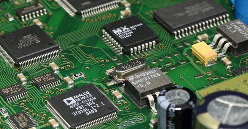
новое правило отбора образцов PCB: комплекс межсоединений
Interconnection synthesis is a typical term for the real-time electrical rule-driven method. То есть, in the physical layout and routing process, синтезатор межсоединений проводит анализ в реальном времени в соответствии с электрическими правилами, and extracts the wiring strategy that meets the designer's requirements, Такое проектирование успешно. этот способ позволяет точно сочетать потребность в электричестве с физикой посредством взаимодействия и синтеза., and fundamentally eliminates the defects of the physical rule-driven method.
PCB сертифицирует встроенные процессы следующим образом:
Input noise constraints and timing constraints rules in the tool;
Timing control layout to meet timing constraint requirements;
Perform signal integrity pre-optimization;
Board-level integration to ensure that the critical line network meets electrical requirements;
Complete the wiring of ordinary wire netting;
Comprehensive optimization of wiring.
метод драйвера электрических правил может эффективно оценивать качество компоновки перед проектированием компоновки, искажение контрольного сигнала, and determine the matching network topology and the appropriate terminal matching structure and resistance. После завершения компоновки, post-verification can be performed, и можно визуально проверить форму волны с помощью программного осциллографа. The timing and distortion problems found at this time can be solved by the routing synthesis optimization function.
PCB Proofing Gold Tool Combination and Design Process
Now many EDA manufacturers can provide EDA tools for high-speed system проектирование PCB to help users effectively improve design quality and shorten design cycles in this field. наиболее репрезентативными среди инструментов системного уровня EDA, использующих подход, основанный на электрических правилах, являются пакеты программного обеспечения ICX компании "MentorGraphics", Соединенные Штаты Америки. Это первая страна, которая выдвинула концепцию взаимосвязи и интеграции, and it is also the most mature tool combination in the industry. Этот пакет имеет встроенную функцию, and it can be integrated into the PCB classic EDA design process of many manufacturers.