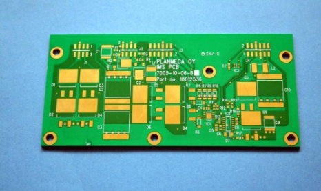
The surface treatment technology of PCB circuit board refers to the process of artificially forming a surface layer on the PCB components and electrical connection points that is different from the mechanical, physical and chemical properties of the substrate. Цель заключается в том, чтобы обеспечить хорошую свариваемость или электрические характеристики PCB.. Because copper tends to exist in the form of oxides in the air, серьезное влияние на свариваемость и электрические характеристики PCB, it is necessary to perform surface treatment on the PCB.

общие поверхностные методы:
выравнивание горячего дутья
The process of coating molten tin-lead solder on the surface of the PCB and leveling (blowning) with heated compressed air to form a coating layer that is resistant to copper oxidation and provides good solderability. когда горячий воздух меняется в обычное время, the solder and copper form a copper-tin metal compound at the junction, его толщина около 1 - 2 мм;
органическая устойчивость к окислению (ОСП)
On the clean bare copper surface, химически выращивать слой органической пленки. This layer of film has anti-oxidation, термосейсмостойкость, and moisture resistance to protect the copper surface from rusting (oxidation or sulfidation, сорт.) in a normal environment; at the same time, при последующей сварке при высокой температуре необходимо удобно и быстро очищать вспомогательный флюс, чтобы облегчить сварку;
химическое никелирование
A thick layer of nickel-gold alloy with good electrical properties is wrapped on the copper surface and can protect the PCB for a long time. Не похоже на OSP, which is only used as an anti-rust barrier layer, Он может использоваться для долгосрочного использования PCB и получить хорошие электрические свойства. In addition, Он также обладает экологической устойчивостью, которая отсутствует в других процессах обработки поверхности;
4. химическое серебро
Between OSP and electroless nickel/пропитка золотом, the process is simpler and faster. при высокой температуре, humidity and pollution, Он по - прежнему может обеспечивать хорошие электрические характеристики и сохраняет хорошую свариваемость, but it will lose its luster. Потому что под слоем серебра нет никеля, immersion silver does not have all the good physical strength of electroless nickel/пропитка золотом;
гальваническое никеля
The conductor on the PCB surface is electroplated with a layer of nickel and then electroplated with a layer of gold. Основная цель никелирования - предотвратить распространение золота и меди. There are two types of electroplated nickel gold: soft gold plating (pure gold, gold indicates that it does not look bright) and hard gold plating (the surface is smooth and hard, wear-resistant, кобальт и другие элементы, and the surface looks brighter). Soft gold is mainly used for gold wire during chip packaging; hard gold is mainly used for electrical interconnection (such as gold fingers) in non-welded areas.
6. технология обработки гибридных поверхностей PCB
Choose two or more surface treatment methods for surface treatment. The common forms are: Immersion Nickel Gold + Anti-oxidation, Electroplating Nickel Gold + Immersion Nickel Gold, Electroplating Nickel Gold + Hot Air Leveling, Immersion Nickel Gold + Hot Air Leveling .
из всех методов обработки поверхности наиболее распространенным и доступным методом является воздушная очистка (без свинца / свинца), однако внимание обращается на правила ЕС, касающиеся рохс.
The above is an introduction to the complete set of PCB circuit board surface treatment methods. Ipcb также предоставляет Производители PCB and PCB manufacturing technology