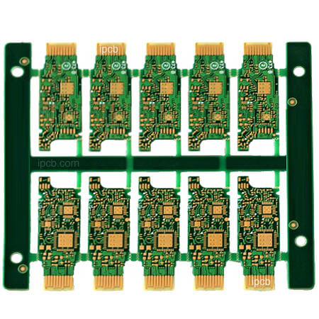
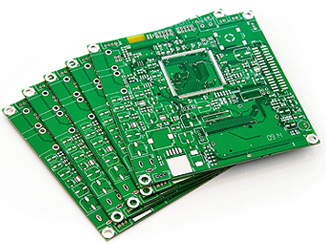
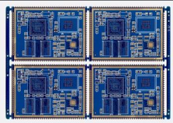
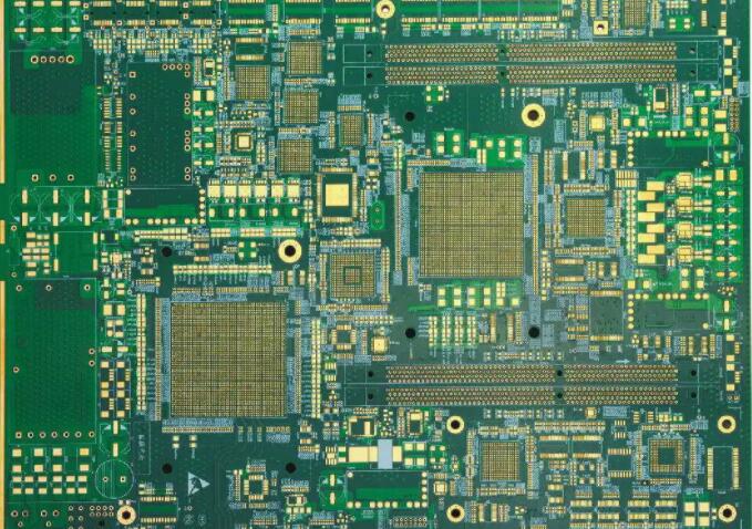
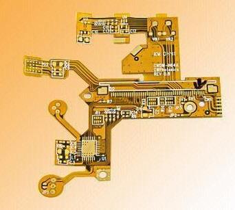
Печатная плата, также известная как печатная плата, может реализовать соединение и функциональность цепей между электронными элементами, а также является важной частью проектирования силовых цепей. сегодня в этой статье мы познакомимся с основными правилами разводки печатной платы и проводки.

Основные правила компоновки компонентов
1.Схема по модулю схемы, связанные схемы, реализующие одну и ту же функцию, называются модулем, принцип близости и централизации элементов в модуле схемы, а цифровая схема и аналоговая схема должны быть разделены;
2.Не монтировать сборку и оборудование на 1 дюйм.27 мм вокруг немонтажных отверстий, таких как позиционные отверстия и стандартные отверстия, не монтировать виджет в течение 3 часов.5 мм (для M2.5) и 4 мм (для M3) вокруг монтажных отверстий, таких как винты;
3.Не вставляйте сквозное отверстие под горизонтально установленные резисторы и другие компоненты, индуктивности (вставные) и электролитические конденсаторы, чтобы избежать короткого замыкания между сквозным отверстием и корпусом компонента после пайки волной припоя.;
4.Расстояние между внешней стороной компонента и краем платы составляет 5 мм;
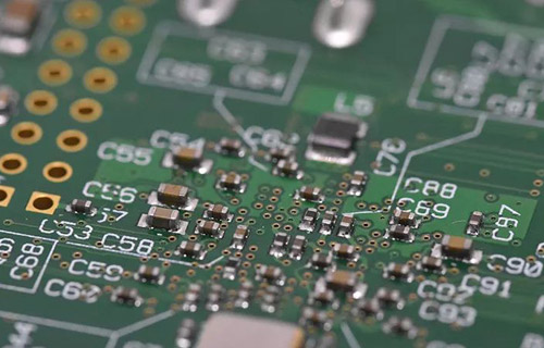
5.Расстояние между внешней стороной площадки установленного компонента и внешней стороной соседнего компонента составляет более 2 мм;
6.Металлические компоненты оболочки и металлические детали (экранирующие коробки, сорт.) не могут касаться других компонентов и не могут находиться рядом с печатными линиями и площадками, расстояние должно быть больше 2мм. Размер монтажных отверстий крепи, эллиптических отверстий и других квадратных отверстий в пластине превышает 3 мм от края пластины;
7.Нагревательный элемент не должен находиться близко к проволоке и термоэлементу; высоконагревательный элемент должен быть равномерно распределен;
8.Розетка должна быть установлена по мере возможности вокруг печатной доски, шинный зажим, связанный с розеткой, должен быть расположен на одной стороне. Особое внимание следует обратить на то, чтобы розетки и другие паяные разъемы не располагались между разъемами, Для удобства сварки этих розеток и соединителей, а также на конструкцию и обвязку силовых кабелей. Расстояние между силовыми розетками и сварочными разъемами должно быть таким, чтобы облегчить установку и извлечение силовых штекеров;
9.Расположение других компонентов: Все компоненты ИС выравниваются по одной стороне, метка полярных компонентов, а маркировка полярности на одной печатной плате не должна быть более чем двух направлений. При появлении двух направлений, два направления перпендикулярны друг другу;
10.Проводка на плате должна иметь надлежащую плотность. При больших различиях плотности, она должна быть заполнена сетчатой медной фольгой, а ячейка должна быть больше 8 мил (или 0.2 мм);
11.Непроницаемое отверстие на вкладке, во избежание потери флюса и. Важные сигнальные линии не должны проходить между контактами разъема;
12.патчи выровнены в одну сторону, направление роли одинаково, а направление упаковки одинаково;
13.Для оборудования полярности направление маркировки полярности на одной плате должно быть как можно более последовательным.
Правила подключения компонентов
В области, где зона разводки находится на расстоянии 1 мм от края печатной платы, монтажное отверстие в пределах 1 мм, разводка запрещена; 2. Линия питания должна быть как можно шире и не должна быть меньше 18 мил; ширина сигнальной линии не должна быть меньше 12 мил; cpu Входящие и исходящие линии не должны быть меньше 10 мил (или 8 мил); расстояние между линиями не должно быть меньше 10 мил; 3, нормальное сквозное отверстие не должно быть меньше 30 мил; 4, двухрядный прямой разъем: прокладка 60mil, отверстие 40mil; 55mil (0805 поверхностный монтаж); 62mil прокладка, 42mil отверстие при подключении непосредственно; безэлектродный конденсатор: 51*55mil (0805 поверхностный монтаж);50mil прокладка, 28mil отверстие при подключении непосредственно; 5. Обратите внимание,что линии электропитания и заземления должны быть как можно более радиоактивными,а сигнальная линия не может иметь обратного хода.
Следующие системы должны уделять особое внимание защите от электромагнитных помех:
(1) Тактовая частота микроконтроллера особенно высока, а скорость движения автобуса особенно высока..
(2) Система содержит мощные, сильноточные цепи, такие как искрогенераторные реле, сильноточный автоматический выключатель и т.д.
(3) Система со схемой слабого аналогового сигнала и высокоточной схемой преобразования АЦП.
Чтобы повысить устойчивость системы к электромагнитным помехам, примите следующие меры:
(1) Выберите микроконтроллер с низкой частотой: Выбор микроконтроллера с низкой частотой внешнего генератора может эффективно снизить уровень шума и улучшить защиту системы от помех. Квадратные и синусоидальные волны одинаковой частоты, высокочастотный состав в квадратичной волне гораздо больше синусоидальной волны. Хотя амплитуда высокой частота квадратичная составляющая, тем выше частота, чем легче его запустить и стать источником шума. Влиятельный высокий частота шума, создаваемого микроконтроллером, примерно в 3 раза выше тактовой частоты.
(2) уменьшение числа микрорегуляторов искажений при передаче сигналов производится главным образом с помощью высокоскоростной технологии CMOS. статический входной ток на входе сигнала составляет около 1 мA, входная емкость - около 10 ПФ, входное сопротивление довольно высокое, выход на высокоскоростную цепь CMOS имеет значительную нагрузку,т.е.значительное выходное значение. когда длинная линия вводится в конец ввода, проблемы с рефлектором очень серьезные, входное сопротивление относительно высокое,что приведет к искажению сигнала и увеличению шумов системы. когда тpd > TRT,он становится проблемой линии передачи, необходимо учитывать такие вопросы, как отражение сигнала и согласование сопротивлений.время задержки сигнала на печатных платах связано с характерным сопротивлением провода, т.е. можно грубо предположить, что скорость передачи сигнала на выводе печатной плиты составляет примерно одну треть одну вторую. в системе, состоящей из микроконтроллеров, обычный логический телефонный элемент TR (стандартное время задержки) находится в диапазоне от 3 до 18 НС.на печатных платах сигнал проходит через резистор 7W и длинный провод 25cm, время задержки в режиме онлайн составляет от 4 до 20нс.То есть,чем короче сигнальный провод на печатных схемах,тем лучше, тем длиннее он не должен превышать 25 См. количество перерывов должно быть как можно меньше,не более двух. когда время нарастания сигнала быстрее,чем время задержки сигнала, по скоростной электронике производится его обработка. при этом следует учитывать совпадение сопротивлений линии передачи.для передачи сигналов между интегральными блоками на печатных платах необходимо избегать ситуации Td > TRD. Чем больше печатные платы, тем медленнее будет система.опыт проектирования печатных плат обобщается следующим образом: время задержки передачи сигналов на печатных платах не должно превышать время номинальной задержки используемого оборудования.
(3) Уменьшение помех между сигнальными линиями:
Ступенчатый сигнал с временем нарастания Tr в точке A передается на клемму B через провод AB. Время задержки сигнала на линии АВ равно Td. В точке D, вследствие прямой передачи сигнала в точке A, отражение сигнала после точки в и задержка линии ав, страничный импульсный сигнал с шириной Tr поддается индукции через время Td. в точке C, в результате прохождения и отражения сигнала на AB,положительный импульсный сигнал, ширина которого в два раза превышает время задержки сигнала линии ав, То есть, 2Td, будут индуцированы. Это перекрестная интерференция между сигналами.интенсивность сигнала помехи связана с di/сигнал в точке C, расстояние между линиями. когда две сигнальные линии не длинны,то,что на самом деле видно на АВ, - это суперпозиция двух импульсов. Микроконтроллер с высоким входным сопротивлением, резким звуком и высокой помехоустойчивостью.На цифровые схемы накладывается 100~200 мВ шума, не влияющего на их работу. Если линия AB на рисунке является аналоговым сигналом, Такие помехи недопустимы. Например, если печатная плата, одна из которых имеет большую площадь заземления, или двухсторонняя плата, когда обратная сторона сигнальной линии заземлена с большой площадью, перекрестные помехи между такими сигналами станут меньше. Причина в том, что большое заземление уменьшает характеристический импеданс сигнальной линии, и отражение сигнала на D-конце значительно уменьшается. Характеристический импеданс обратно пропорционален квадрату диэлектрической проницаемости среды между сигнальной линией и землей, а это прямая зависимость от толщины диэлектрика. Если линия AB является аналоговым сигналом, во избежание интерференции цифровой схемы сигнальная линия CD на AB, поверхность под линией AB, и расстояние от линии AB до линии CD должно быть больше, чем 2 ~ 3 раза расстояние между линией AB и землей. Экранирующая часть используется, и провода заземления расположены на левой и правой стороне свинца на стороне со стыком свинца.
(4) Уменьшите шум от источника питания Поставляя энергию в систему, источник также вносит в нее шум. Линия сброса, линия прерывания и другие линии управления микроконтроллера в схеме легко нарушаются внешними шумами. фазовый сдвиг фазового сдвига, и даже в системах с батарейным питанием сама батарея является высокочастотным шумом. аналоговый сигнал в схеме более восприимчив к шуму от источника.
(5) Обращайте внимание на высокие частотные характеристики печатных плат и компонентов. В случае высокой частоты нельзя игнорировать выводы, межслойные соединения, резисторы, конденсаторы, а также распределенную индуктивность и емкость разъемов на печатной плате. Распределенную индуктивность конденсатора нельзя игнорировать, а распределенную емкость индуктора нельзя игнорировать. Сопротивление будет отражать высокую частоту сигнала, распределенная емкость проводов сработает. Когда длина больше 1/частота шумов соответствует длине волны 20, возникает эффект антенны, шум пройдет по проводам.Провода печатной платы вызывают емкость около 0,6 пф. Упаковочный материал интегральной схемы сам по себе вносит емкость 2~6пф. В разъем на плате с распределенной индуктивностью 520nH. В двухрядный прямой 24-контактный держатель интегральной схемы вводится распределенная индуктивность 4 ~ 18nH. Этими малыми параметрами распределения можно пренебречь для данной линейки микроконтроллеров на низких частотах; особое внимание следует уделить высокоскоростным системам.
(6) Расположение компонентов должно быть разумно разделено. Расположение компонентов на печатной плате должно быть полностью продумано с точки зрения защиты от электромагнитных помех. Один из принципов заключается в том, что провод между сборками должен быть как можно короче. При компоновке блок аналоговых сигналов, часть высокоскоростных цифровых схем и часть источников шума (таких как реле, сильноточные переключатели и т. д.) должны быть разумно разделены, Поэтому сигнал между ними должен быть. Обращайтесь с проводом заземления на печатной плате, важное значение имеют линии электропитания и заземления. Чтобы преодолеть электромагнитные помехи, Основным средством является заземление.
Двухсторонняя панель, расположение провода заземления очень конкретный. метод одноточечного заземления, источник питания и земли подключены к печатной плате с обоих концов источника питания, контакт используется для питания, контакт используется для заземления. На печатной плате заземление через несколько цепей, и они будут собраны на контакте обратного источника питания, Это называется одноточечное заземление. так называемый аналоговый отрыв, цифровая земля, И высокая мощность заземления означает, что провода разделены, и все они собраны вместе в этой точке заземления. сигнал при подключении к непечатной схеме, экранированный кабель. Для высокочастотных и цифровых сигналов - концевое заземление экранированного кабеля. Экранированные кабели для низкочастотных аналоговых сигналов должны быть заземлены с одного конца. цепи, очень чувствительные к шумам и помехам, или особенно чувствительные к шумам и помехам высокочастотные помехи на плате печатной платы должны быть экранированы металлическим кожухом.