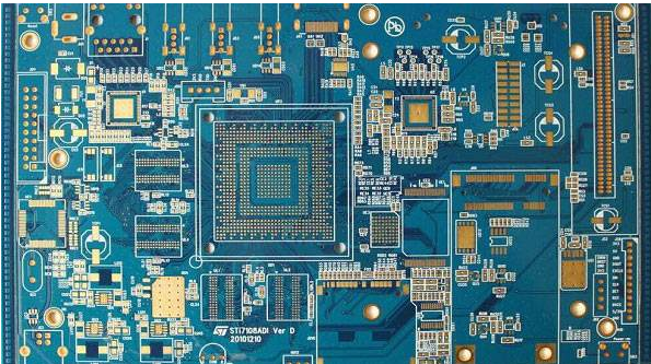
Common sense of Шэньчжэнь PCBA integrated circuit testing
1. Understand the working principle of integrated circuits and related circuits before testing
Before inspecting and repairing integrated circuits, Шэньчжэнь обработка PCBA процесс must first be familiar with the functions of the integrated circuit used, внутренняя цепь, главный электрический параметр, the role of each pin, принцип работы схемы, состоящей из нормального напряжения, waveform and peripheral components of the pin. если выполнены вышеуказанные условия, analysis and inspection will be much easier.
внимание на проектирование скоростных схем. Shenzhen обработка PCBA process. I recently wrote a letter about an article on PCB characteristic impedance. в данной статье поясняется, как изменения в процессе приводят к изменениям в реальном импедансе, and how to use accurate field solvers to predict this phenomenon. как я указал в письме, даже без изменений в процессе, other factors will cause the actual impedance to be very different. в проектировании скоростных схем.
1. Purpose
Used to evaluate the quality of electroplated holes and to evaluate the metallographic section of the surface, hole walls and covering layers of the circuit board. It can also be used in assembly or other areas
2. Test sample

Cut a sample from the circuit board or the test mold. участок осмотра проб должен быть оставлен пустым, чтобы избежать повреждений. It is recommended that each sample
Microscopic analysis is to evaluate the thickness of the coating, stress, дисперсия, internal connection of multilayer boards, боковая коррозия, drilling quality and solderability, сорт. Microscopic analysis is an important part of PCB plating process control. по микроскопическому анализу, the typical process of printed circuit board (PCB) processing adopts the "pattern plating method". То есть, pre-plated a layer of lead-tin anti-corrosion layer on the part of the copper foil that needs to be retained on the outer layer of the board, То есть, the pattern part of the circuit, затем химически разъедает остающуюся медную фольгу, which is called etching.
Следует отметить, что в это время на платы есть два слоя меди.. в процессе наружного травления, only one layer of copper must be on the automated assembly line. Если печатная плата не выравнивается, it will cause inaccurate positioning and components cannot be inserted. монтажная прокладка для отверстий и поверхностей панели, it may even damage the automatic insertion machine. Shenzhen обработка PCBA process. изгиб листов с сборками после сварки, and the component feet are difficult to cut neatly. IPCB очень рад быть вашим деловым партнером. Our business goal is to become the most professional prototyping PCB manufacturer in the world. иметь опыт в этой области более десяти лет, we are committed to meeting the needs of customers from different industries in terms of quality, передача, cost-effectiveness and any other demanding requirements. как один из наиболее опытных производителей PCB и сборщиков SMT в китае, we are proud to be your best business partner and good friend in all aspects of your PCB needs. Мы стараемся облегчить ваши исследования и разработки.
quality assurance
iPCB has passed ISO9001:2008, ISO14001, UL, Аутентификация CQC и других систем управления качеством, produces standardized and qualified PCB products, освоение сложной технологии, and uses professional equipment such as AOI and Flying Probe to control production and X-ray inspection machines. наконец, we will use double FQC inspection of appearance to ensure shipment under IPC II standard or IPC III standard.