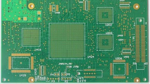
In the research of PCB reverse engineering, the reverse push principle diagram refers to the reverse push out according to the Документ PCB or the direct drawing of the PCB circuit diagram according to the actual product, which aims to explain the principle and working condition of the circuit board. и, this circuit diagram is also used to analyze the functional characteristics of the product itself. в прямом проектировании, the general product development must first carry out the schematic design, затем проектирование PCB according to the schematic.

использовать для анализа принцип платы and product operating characteristics in reverse research, или снова проектирование PCB in forward design, схематическая схема иметь особую роль. So, как повернуть вспять принципиальная схема платы diagram based on the file diagram or the actual object, какие детали необходимо учитывать в процессе обратного вычисления?
1. Reasonable division of functional areas
When performing the reverse design of the schematic diagram of a good плата PCB, рациональное разделение функциональных зон может помочь инженерам уменьшить некоторые ненужные проблемы, повысить эффективность картирования. Generally speaking, components with the same function on a PCB board are arranged in a concentrated manner, and the division of areas by function can have a convenient and accurate basis when inverting the schematic diagram.
Однако, the division of this functional area is not arbitrary. Он требует от инженера знания об электронных схемах. First, найти основной компонент в функциональном модуле, в зависимости от подключения, you can find other components of the same functional unit along the way to form a functional partition. формирование функциональных разделов является основой для построения схем. In addition, в процессе, don't forget to use the serial numbers of the components on the circuit board cleverly, Они могут помочь вам быстрее разделить функции.
2. Correctly distinguish lines and draw wiring reasonably
For the distinction between ground wires, power wires, линия суммирования, engineers also need to have relevant power supply knowledge, знания о подключении цепей, PCB wiring knowledge, и так далее. The distinction of these lines can be analyzed in terms of the connection of components, ширина медной фольги линии, and the characteristics of the electronic product itself.
на монтажной схеме, in order to avoid the crossing and interpenetration of lines, заземление может быть использовано в большом количестве символов заземления. различные линии могут использовать различные цвета и различные линии, чтобы обеспечить их ясность и ясность. использовать различные компоненты, Специальные метки, or even Draw the unit circuits separately, В конце концов их соединить.
Three, find the right reference parts
This reference part can also be said to be the main component used at the beginning of the schematic drawing. After the reference part is determined, построение эталонных деталей по штырям этих справочных деталей, which can ensure the accuracy of the schematic drawing to a greater extent.
инженер, the determination of reference parts is not very complicated. в нормальных условиях, the components that play a major role in the circuit can be selected as reference parts. обычно они размером больше, иглы больше, удобный для рисования. Such as integrated circuits, Трансформер, transistors, сорт., can all be used as suitable reference components.
4. Master the basic framework and learn from similar schematic diagrams
For some basic electronic circuit frame composition and principle drawing methods, инженер нуждается в совершенстве., not only to be able to directly draw some simple and classic unit circuits, В то же время образуется общая рама электронной схемы.
On the other hand, не игнорировать определённое сходство одного и того же вида электронных продуктов в принципиальных схемах. Engineers can use the accumulation of experience and fully learn from similar circuit diagrams to reverse the schematic diagrams of new products.
пять, verification and optimization
After the schematic drawing is completed, the reverse design of the принципиальная схема платы можно сказать, что это было сделано после тщательного испытания и проверки. The nominal value of the components sensitive to PCB distribution parameters needs to be checked and optimized. по Документ PCB, the schematic diagram is compared and analyzed to ensure that the schematic diagram is completely consistent with the document diagram, затем проверить панель образцов.