

")
Shape: max. 100 mm × 100 mm
Line width / spacing: min.0.075mm/0.15mm
Printed conductor thickness: 10 ~ 25 μ M
Printing line width accuracy: ± 10 μ M
Stack alignment accuracy: ≤ 30 μ M
Through hole diameter: min.0.1mm
Sintering shrinkage accuracy: ± 0.2%
Distance between conductor and shape edge: min.0.2mm
Distance between metal through hole and line: min.0.15mm
Overlap distance of resistance / Conductor: min.0.15mm
Resistance size: min.0.15mm × 0.15mm
Total number of media layers: ≤ 40 layers
Application : Filter PCB, diplexer PCB, LTCC chip antenna PCB
LTCC ceramic substrate technology is a three-dimensional integration technology of complex microwave and digital circuits by using new ceramic materials and microwave thick film integration technology. With the rapid development of monolithic integrated technology, the integration of active devices is getting higher and higher, reaching an unprecedented level, which makes the integration of passive devices very important. LTCC technology can meet the integration requirements of passive devices such as resistor, capacitor, inductor, filter and coupler.
The resistance of LTCC substrate is 10 Ω, 100 Ω, 1K Ω and 10K Ω respectively. The accuracy of surface resistance adjustment method is less than 1%, and the accuracy of internal embedded resistance is less than 30%. Other passive devices can be designed according to the relevant material parameters. LTCC substrate can be multi-layer wiring, up to 40 layers.
")
Low Temperature Co-fired Ceramic PCB(LTCC PCB)
In recent years, ceramic substrate technology has developed rapidly, especially on the basis of traditional ceramic substrate, high-temperature co fired ceramic substrate and low-temperature CO fired ceramic substrate have been developed, which makes the ceramic substrate in the high-density assembly of high-power circuits get a deeper and wider application. Low temperature co fired multilayer substrate is a newly developed micro assembly substrate, which concentrates the advantages of thick film process and high temperature co firing. In more than ten years, this kind of substrate has been developed rapidly. As a high density, high speed circuit board, it is widely used in computer, communication, missile, rocket, radar and other fields. For example, Dupon company of the United States uses 8-layer low temperature co fired multilayer substrate in the test circuit of stinger missile. Fujitsu of Japan uses 61 layers of low temperature co fired ceramic substrate to make multi chip module of vp2000 series supercomputer, while NEC company has made 78 layers of low temperature co fired multi-layer substrate with an area of 225 * 225 square mm. It contains 11540 I / O terminals and can install up to 100 VLSI chips.
Low temperature co fired multilayer ceramic substrate is made of many single ceramic substrates. Each ceramic substrate consists of a layer of ceramic materials and conductive circuits attached to the ceramic layer, which is usually called the conduction band. The through holes of the ceramic layer are filled with conductive materials. It connects the conduction band lines in different ceramic layers to form a three-dimensional circuit network. The IC chip is installed on the top layer of multilayer ceramics. The integrated block is welded with the circuit in the multilayer ceramic substrate through pins to form an interconnection circuit. The metal conductive layer on the surface of the substrate is formed in advance during the sintering process of the ceramic substrate, and there are needle shaped terminals at the bottom of the substrate. In this way, the co fired multilayer ceramic substrate is used to assemble the micro components to form a three-dimensional structure with high density, high speed and high reliability.

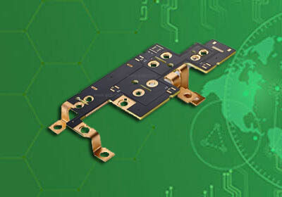
Typical structure of LTCC ceramic PCB
Compared with other PCB technologies, LTCC PCB has many advantages
1. Ceramic materials have excellent characteristics of high frequency, high speed transmission and wide passband. The dielectric constant of LTCC materials can vary in a wide range according to the different ingredients. The use of metal materials with high conductivity as conductor materials can improve the quality factor of circuit system and increase the flexibility of circuit design;
2. It can adapt to the requirements of high current and high temperature resistance, and has better thermal conductivity than ordinary PCB circuit board. It greatly optimizes the heat dissipation design of electronic equipment, with high reliability, and can be applied to harsh environment and prolong its service life;
3. The circuit board with a high number of layers can be fabricated, and multiple passive components can be embedded in it, which can avoid the cost of packaging components. On the three-dimensional circuit board with high layers, passive and active integration can be realized, which is conducive to improving the assembly density of the circuit and further reducing the volume and weight;
4. It has good compatibility with other multi-layer wiring technologies, for example, the combination of LTCC and thin-film wiring technology can achieve higher assembly density and better performance of hybrid multi-layer substrate and hybrid multi-chip module;
5. The discontinuous production process is convenient for the quality inspection of each layer of wiring and interconnection holes before the finished product is made, which is conducive to improving the yield and quality of multilayer substrate, shortening the production cycle and reducing the cost.
6. Energy saving, material saving, green and environmental protection have become an irresistible trend in the development of the component industry. LTCC also caters to this development demand and reduces the environmental pollution caused by raw materials, wastes and production process to the greatest extent.
Shape: max. 100 mm × 100 mm
Line width / spacing: min.0.075mm/0.15mm
Printed conductor thickness: 10 ~ 25 μ M
Printing line width accuracy: ± 10 μ M
Stack alignment accuracy: ≤ 30 μ M
Through hole diameter: min.0.1mm
Sintering shrinkage accuracy: ± 0.2%
Distance between conductor and shape edge: min.0.2mm
Distance between metal through hole and line: min.0.15mm
Overlap distance of resistance / Conductor: min.0.15mm
Resistance size: min.0.15mm × 0.15mm
Total number of media layers: ≤ 40 layers
Application : Filter PCB, diplexer PCB, LTCC chip antenna PCB
For PCB technical problems, iPCB knowledgeable support team is here to help you with every step. You can also request PCB quotation here. Please contact E-mail sales@ipcb.com
We will respond very quickly.


